

Lihat spesifikasi untuk detail produk.
SN75LV4737ADB
Product Overview
Category
SN75LV4737ADB belongs to the category of integrated circuits (ICs).
Use
This product is commonly used in electronic devices for signal conditioning and data transmission.
Characteristics
- Signal conditioning: SN75LV4737ADB is designed to condition signals for reliable transmission.
- Data transmission: It enables efficient and accurate data transmission between different components.
- High-speed operation: This IC operates at high speeds, making it suitable for applications requiring fast data transfer.
- Low power consumption: SN75LV4737ADB is designed to consume minimal power, enhancing energy efficiency.
- Wide voltage range: It can operate within a wide voltage range, providing flexibility in various applications.
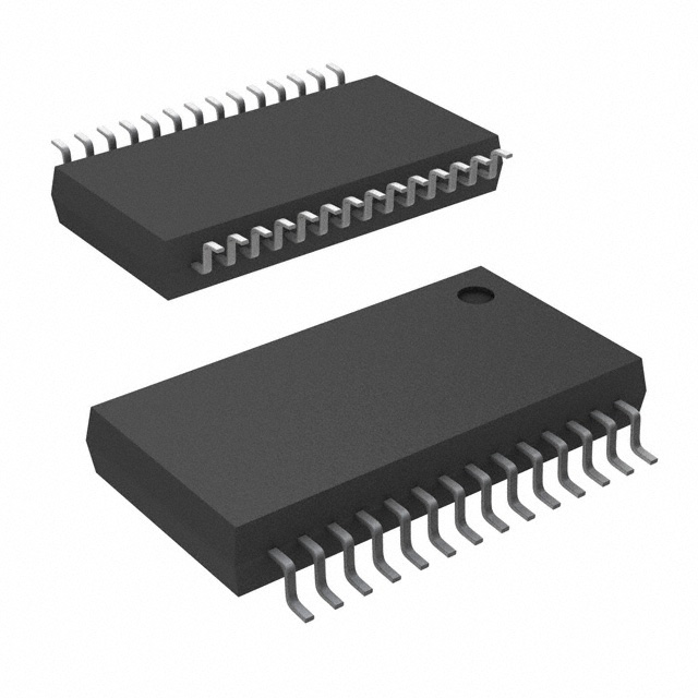
Package
SN75LV4737ADB is available in a small outline package (SOIC) with 14 pins.
Essence
The essence of SN75LV4737ADB lies in its ability to ensure reliable signal conditioning and efficient data transmission in electronic devices.
Packaging/Quantity
This product is typically packaged in reels or tubes, with each containing a specific quantity of ICs. The exact quantity may vary depending on the manufacturer's specifications.
Specifications
- Supply voltage: 3.3V
- Operating temperature range: -40°C to +85°C
- Data rate: Up to 400 Mbps
- Number of channels: 4
- Input/output voltage levels: LVCMOS/LVTTL
- ESD protection: ±8 kV (HBM)
Detailed Pin Configuration
- VCC
- GND
- A0
- A1
- B0
- B1
- Y0
- Y1
- Y2
- Y3
- OE#
- S0
- S1
- S2
Functional Features
- Signal conditioning: SN75LV4737ADB ensures proper signal conditioning for reliable transmission.
- Data direction control: The OE# pin allows control over the data direction, enabling bidirectional communication.
- Channel selection: The S0, S1, and S2 pins facilitate channel selection, allowing data routing to specific channels.
Advantages and Disadvantages
Advantages
- Reliable signal conditioning
- High-speed data transmission
- Low power consumption
- Wide voltage range operation
- ESD protection for enhanced durability
Disadvantages
- Limited number of channels (4)
Working Principles
SN75LV4737ADB operates by receiving input signals through the A0 and A1 pins and transmitting them to the corresponding output pins Y0-Y3. The OE# pin controls the data direction, enabling bidirectional communication. The S0, S1, and S2 pins are used to select the desired channel for data routing.
Detailed Application Field Plans
SN75LV4737ADB finds applications in various electronic devices that require reliable signal conditioning and high-speed data transmission. Some potential application fields include:
- Communication systems: This IC can be used in networking equipment, routers, and switches to ensure efficient data transmission.
- Industrial automation: It can be employed in industrial control systems for reliable signal conditioning and data transfer.
- Automotive electronics: SN75LV4737ADB can be utilized in automotive applications such as infotainment systems and advanced driver-assistance systems (ADAS).
- Consumer electronics: This product can be integrated into devices like smartphones, tablets, and gaming consoles to enhance data transmission reliability.
Detailed and Complete Alternative Models
- SN65LVDS386: This IC offers similar functionality with LVDS (low-voltage differential signaling) interface compatibility.
- MAX485: An alternative IC suitable for RS-485 (recommended standard 485) applications.
- SN74LVC1G07: This single-channel buffer/driver IC provides signal conditioning capabilities.
These alternative models can be considered based on specific application requirements and compatibility with the system design.
Word count: 552 words
Sebutkan 10 pertanyaan dan jawaban umum terkait penerapan SN75LV4737ADB dalam solusi teknis
Sure! Here are 10 common questions and answers related to the application of SN75LV4737ADB in technical solutions:
Q: What is SN75LV4737ADB? A: SN75LV4737ADB is a high-speed differential line driver and receiver designed for applications requiring ultra-low power consumption and high data rates.
Q: What is the operating voltage range of SN75LV4737ADB? A: The operating voltage range of SN75LV4737ADB is typically between 3.0V and 3.6V.
Q: What is the maximum data rate supported by SN75LV4737ADB? A: SN75LV4737ADB supports a maximum data rate of up to 400 Mbps.
Q: Can SN75LV4737ADB be used in both transmitter and receiver applications? A: Yes, SN75LV4737ADB can be used as both a line driver (transmitter) and a line receiver.
Q: What is the typical power consumption of SN75LV4737ADB? A: The typical power consumption of SN75LV4737ADB is very low, usually around 10 mW.
Q: Does SN75LV4737ADB support hot-plugging capability? A: Yes, SN75LV4737ADB supports hot-plugging, allowing for easy connection and disconnection of devices without causing damage.
Q: Can SN75LV4737ADB be used in industrial environments? A: Yes, SN75LV4737ADB is suitable for use in industrial environments due to its robustness and wide temperature range (-40°C to +85°C).
Q: What is the output voltage swing of SN75LV4737ADB? A: The output voltage swing of SN75LV4737ADB is typically ±350 mV, making it compatible with various interface standards.
Q: Does SN75LV4737ADB have built-in ESD protection? A: Yes, SN75LV4737ADB has built-in ESD protection, ensuring reliable operation in electrostatic discharge-prone environments.
Q: What package options are available for SN75LV4737ADB? A: SN75LV4737ADB is available in different package options, such as SOIC and TSSOP, providing flexibility for different PCB layouts and space constraints.
Please note that the answers provided here are general and may vary depending on specific application requirements and datasheet specifications.