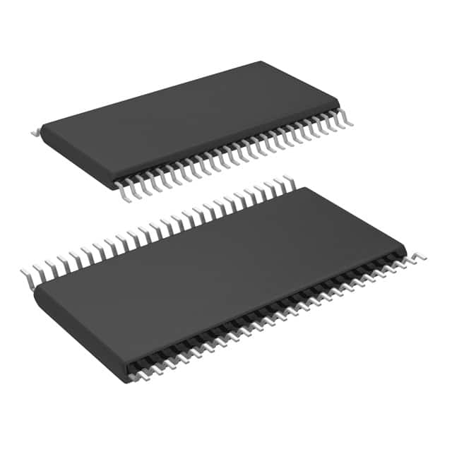
Lihat spesifikasi untuk detail produk.

SN74LVTH162244DGGR
Product Overview
- Category: Integrated Circuit (IC)
- Use: Logic Level Translator
- Characteristics: High-speed, low-voltage, 16-bit buffer/driver with 3-state outputs
- Package: TSSOP (Thin Shrink Small Outline Package)
- Essence: Logic level translation between different voltage domains
- Packaging/Quantity: Tape and Reel, 2500 units per reel
Specifications
- Supply Voltage Range: 2.7V to 3.6V
- Input Voltage Range: 0V to VCC
- Output Voltage Range: 0V to VCC
- Operating Temperature Range: -40°C to +85°C
- Propagation Delay Time: 3.8ns (max) at 3.3V supply
- Output Drive Capability: ±24mA
- ESD Protection: Human Body Model > 2000V
Detailed Pin Configuration
The SN74LVTH162244DGGR has a 48-pin TSSOP package with the following pin configuration:
- OE (Output Enable) 1
- A1 (Input) 1
- Y1 (Output) 1
- GND (Ground)
- Y2 (Output) 2
- A2 (Input) 2
- OE (Output Enable) 2
- VCC (Supply Voltage)
- B1 (Input) 1
- Y3 (Output) 3
- A3 (Input) 3
- B2 (Input) 2
- Y4 (Output) 4
- A4 (Input) 4
- OE (Output Enable) 3
- GND (Ground)
- Y5 (Output) 5
- A5 (Input) 5
- OE (Output Enable) 4
- VCC (Supply Voltage)
- B3 (Input) 3
- Y6 (Output) 6
- A6 (Input) 6
- B4 (Input) 4
- Y7 (Output) 7
- A7 (Input) 7
- OE (Output Enable) 5
- GND (Ground)
- Y8 (Output) 8
- A8 (Input) 8
- OE (Output Enable) 6
- VCC (Supply Voltage)
- B5 (Input) 5
- Y9 (Output) 9
- A9 (Input) 9
- B6 (Input) 6
- Y10 (Output) 10
- A10 (Input) 10
- OE (Output Enable) 7
- GND (Ground)
- Y11 (Output) 11
- A11 (Input) 11
- OE (Output Enable) 8
- VCC (Supply Voltage)
- B7 (Input) 7
- Y12 (Output) 12
- A12 (Input) 12
- B8 (Input) 8
Functional Features
- High-speed operation: The SN74LVTH162244DGGR can operate at high frequencies, making it suitable for applications requiring fast data transmission.
- Logic level translation: It provides bidirectional voltage translation between different voltage domains, allowing communication between devices operating at different logic levels.
- 3-state outputs: The 16-bit buffer/driver has 3-state outputs, enabling multiple devices to share a common bus without interference.
Advantages and Disadvantages
Advantages: - High-speed operation allows for efficient data transfer. - Wide supply voltage range enables compatibility with various systems. - 3-state outputs facilitate bus sharing and reduce signal conflicts.
Disadvantages: - Limited output drive capability may not be suitable for applications requiring high current sourcing or sinking. - The TSSOP package may require careful handling during assembly due to its small size.
Working Principles
The SN74LVTH162244DGGR operates by receiving input signals from one voltage domain and translating them to the corresponding logic levels of another voltage domain. It utilizes a combination of CMOS and TTL technologies to achieve high-speed operation and low-voltage compatibility. The output enable (OE) pins control the tri-state outputs, allowing the device to be effectively connected or disconnected from the bus.
Detailed Application Field Plans
The SN74LVTH162244DGGR is commonly used in various applications, including:
- Microprocessor interfacing: It facilitates communication between microprocessors operating at different logic levels.
- Memory modules: It enables data transfer between memory modules with different voltage requirements
Sebutkan 10 pertanyaan dan jawaban umum terkait penerapan SN74LVTH162244DGGR dalam solusi teknis
Sure! Here are 10 common questions and answers related to the application of SN74LVTH162244DGGR:
Q: What is SN74LVTH162244DGGR? A: SN74LVTH162244DGGR is a 16-bit buffer/driver with 3-state outputs, designed for low-voltage (3.3V) applications.
Q: What is the maximum operating voltage for SN74LVTH162244DGGR? A: The maximum operating voltage for SN74LVTH162244DGGR is 3.6V.
Q: What is the output current capability of SN74LVTH162244DGGR? A: SN74LVTH162244DGGR has a typical output current capability of ±12mA.
Q: Can SN74LVTH162244DGGR be used in bidirectional data transfer applications? A: Yes, SN74LVTH162244DGGR can be used for bidirectional data transfer as it has 3-state outputs.
Q: What is the propagation delay of SN74LVTH162244DGGR? A: The propagation delay of SN74LVTH162244DGGR is typically around 3.8ns.
Q: Is SN74LVTH162244DGGR compatible with TTL and CMOS logic levels? A: Yes, SN74LVTH162244DGGR is compatible with both TTL and CMOS logic levels.
Q: Can SN74LVTH162244DGGR be used in high-speed applications? A: Yes, SN74LVTH162244DGGR is designed for high-speed operation and can be used in such applications.
Q: Does SN74LVTH162244DGGR have built-in ESD protection? A: Yes, SN74LVTH162244DGGR has built-in ESD protection to safeguard against electrostatic discharge.
Q: What is the package type for SN74LVTH162244DGGR? A: SN74LVTH162244DGGR comes in a TSSOP-48 package.
Q: Can SN74LVTH162244DGGR be used in automotive applications? A: Yes, SN74LVTH162244DGGR is qualified for automotive applications and meets the necessary standards.
Please note that these answers are general and may vary depending on the specific datasheet and application requirements.

