

Lihat spesifikasi untuk detail produk.
SN74LVC2G34YZAR
Product Overview
- Category: Integrated Circuit
- Use: Logic Gate
- Characteristics: Dual Buffer/Driver with Open-Drain Outputs
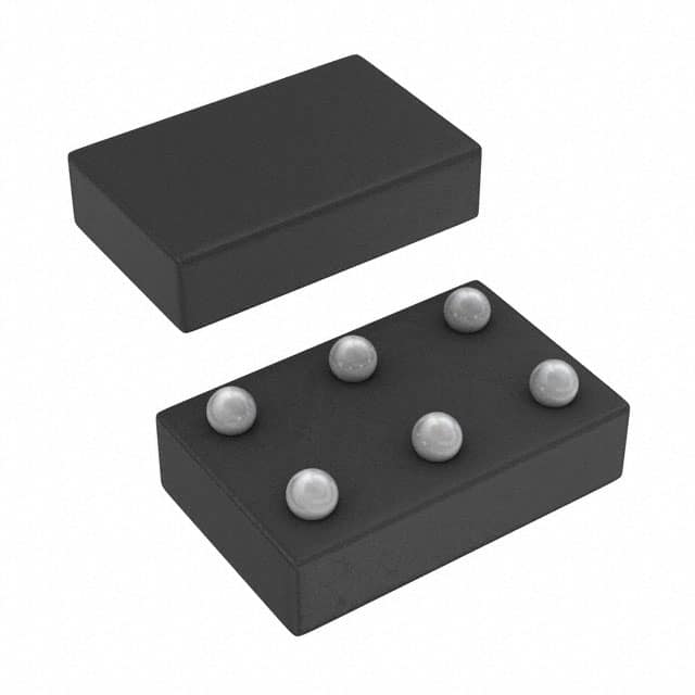
- Package: 8-Bump micro SMD (YZA)
- Essence: This integrated circuit is a dual buffer/driver with open-drain outputs, designed for voltage level translation between different logic levels.
- Packaging/Quantity: Available in tape and reel packaging, with 3000 units per reel.
Specifications
- Supply Voltage Range: 1.65V to 5.5V
- High-Level Input Voltage: 0.7 x VCC
- Low-Level Input Voltage: 0.3 x VCC
- High-Level Output Voltage: 0.9 x VCC
- Low-Level Output Voltage: 0.1 x VCC
- Maximum Operating Frequency: 100 MHz
- Propagation Delay: 4.6 ns (Max) at 3.3V
- Operating Temperature Range: -40°C to +85°C
Detailed Pin Configuration
The SN74LVC2G34YZAR has the following pin configuration:
___________
      |           |
   1 -| A         |
   2 -| B         |
   3 -| Y         |
   4 -| GND       |
   5 -| Y         |
   6 -| B         |
   7 -| A         |
   8 -| VCC       |
      |___________|
Functional Features
- Dual buffer/driver with open-drain outputs
- Provides voltage level translation between different logic levels
- Supports bidirectional data flow
- Allows connection of devices operating at different voltage levels
- Enables interfacing between systems with different voltage requirements
Advantages and Disadvantages
Advantages: - Enables voltage level translation, facilitating communication between devices with different logic levels - Supports bidirectional data flow, allowing for versatile applications - Wide supply voltage range allows compatibility with various systems - Small package size (8-Bump micro SMD) saves board space
Disadvantages: - Limited maximum operating frequency compared to some other logic gates - Propagation delay may affect timing-sensitive applications
Working Principles
The SN74LVC2G34YZAR is a dual buffer/driver with open-drain outputs. It operates by receiving input signals on pins A and B, and providing the corresponding output signals on pins Y. The open-drain outputs allow bidirectional data flow, making it suitable for applications where data needs to be transmitted in both directions.
The integrated circuit performs voltage level translation by converting the input logic levels to the appropriate output logic levels. This enables communication between devices operating at different voltage levels, ensuring compatibility and seamless data transfer.
Detailed Application Field Plans
The SN74LVC2G34YZAR finds applications in various fields, including:
- Microcontrollers and Embedded Systems: Facilitates communication between microcontrollers operating at different voltage levels.
- Industrial Automation: Enables interfacing between different components of industrial automation systems, such as sensors, actuators, and control units.
- Consumer Electronics: Used in devices like smartphones, tablets, and gaming consoles to connect components operating at different voltage levels.
- Automotive Electronics: Supports voltage level translation in automotive systems, allowing different modules to communicate effectively.
- Communication Systems: Used in networking equipment and communication protocols to ensure compatibility between devices with varying voltage requirements.
Detailed and Complete Alternative Models
Some alternative models that provide similar functionality to the SN74LVC2G34YZAR are:
- SN74LVC2G07: Dual Buffer/Driver with Open-Drain Outputs, available in different package options.
- SN74LVC2G17: Dual Schmitt-Trigger Buffer/Driver with Open-Drain Outputs, suitable for applications requiring hysteresis.
- SN74LVC2G241: Dual Buffer/Driver with 3-State Outputs, provides additional control over output states.
These alternative models offer similar voltage level translation capabilities and can be considered based on specific application requirements.
Word count: 536 words
Sebutkan 10 pertanyaan dan jawaban umum terkait penerapan SN74LVC2G34YZAR dalam solusi teknis
Sure! Here are 10 common questions and answers related to the application of SN74LVC2G34YZAR in technical solutions:
Q: What is SN74LVC2G34YZAR? A: SN74LVC2G34YZAR is a dual buffer gate IC (Integrated Circuit) that can be used for voltage level translation and signal buffering.
Q: What is the operating voltage range of SN74LVC2G34YZAR? A: The operating voltage range of SN74LVC2G34YZAR is from 1.65V to 5.5V.
Q: Can SN74LVC2G34YZAR be used for bidirectional level shifting? A: No, SN74LVC2G34YZAR is a unidirectional buffer gate and cannot be used for bidirectional level shifting.
Q: What is the maximum output current of SN74LVC2G34YZAR? A: The maximum output current of SN74LVC2G34YZAR is typically 32mA.
Q: Can SN74LVC2G34YZAR be used with both CMOS and TTL logic levels? A: Yes, SN74LVC2G34YZAR is compatible with both CMOS and TTL logic levels.
Q: What is the propagation delay of SN74LVC2G34YZAR? A: The propagation delay of SN74LVC2G34YZAR is typically around 3.7ns.
Q: Can SN74LVC2G34YZAR be used for level shifting between different voltage domains? A: Yes, SN74LVC2G34YZAR can be used for level shifting between different voltage domains, as long as the voltage levels are within its operating range.
Q: Does SN74LVC2G34YZAR have built-in ESD protection? A: Yes, SN74LVC2G34YZAR has built-in ESD (Electrostatic Discharge) protection to safeguard against electrostatic damage.
Q: What is the package type of SN74LVC2G34YZAR? A: SN74LVC2G34YZAR is available in a small SOT-553 package.
Q: Can SN74LVC2G34YZAR be used in high-speed applications? A: Yes, SN74LVC2G34YZAR can be used in high-speed applications as it has a maximum frequency rating of 100MHz.
Please note that these answers are general and may vary depending on specific datasheet specifications and application requirements.