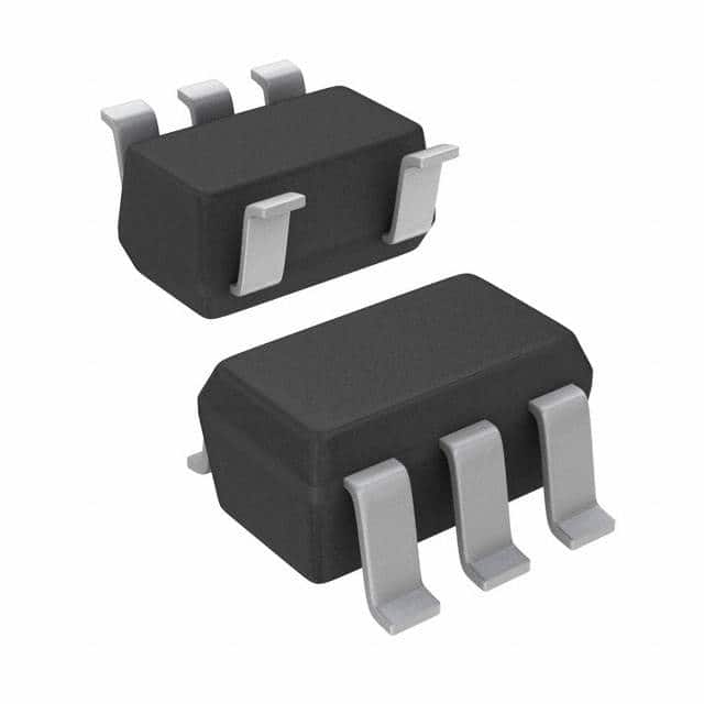
Lihat spesifikasi untuk detail produk.

SN74LVC1G08QDBVRQ1
Product Overview
- Category: Integrated Circuit (IC)
- Use: Logic Gate
- Characteristics: Single 2-input AND gate
- Package: SOT-23-5
- Essence: High-speed CMOS technology
- Packaging/Quantity: Tape and Reel, 3000 pieces per reel
Specifications
- Supply Voltage Range: 1.65V to 5.5V
- Input Voltage Range: 0V to VCC
- Output Voltage Range: 0V to VCC
- High-Level Input Voltage: 0.7 x VCC
- Low-Level Input Voltage: 0.3 x VCC
- High-Level Output Voltage: 0.9 x VCC
- Low-Level Output Voltage: 0.1 x VCC
- Propagation Delay: 4.3 ns (typical)
- Operating Temperature Range: -40°C to +125°C
Detailed Pin Configuration
The SN74LVC1G08QDBVRQ1 has a total of 5 pins:
- GND (Ground): Connected to the ground reference potential.
- A (Input A): First input for the AND gate.
- B (Input B): Second input for the AND gate.
- Y (Output): Output of the AND gate.
- VCC (Supply Voltage): Connected to the positive supply voltage.
Functional Features
- Single 2-input AND gate functionality.
- High-speed operation due to advanced CMOS technology.
- Wide operating voltage range allows compatibility with various systems.
- Low power consumption.
- Schmitt-trigger inputs provide hysteresis for improved noise immunity.
- Supports mixed-mode voltage operation.
Advantages and Disadvantages
Advantages: - Compact size and low power consumption make it suitable for portable devices. - High-speed operation enables efficient data processing. - Wide operating voltage range allows compatibility with different power supply levels. - Schmitt-trigger inputs enhance noise immunity.
Disadvantages: - Limited to a single 2-input AND gate functionality. - Not suitable for applications requiring more complex logic operations.
Working Principles
The SN74LVC1G08QDBVRQ1 is a CMOS-based logic gate that implements the AND function. It operates by receiving two input signals, A and B, and producing an output signal, Y, which is the logical AND of the inputs. The gate utilizes high-speed CMOS technology, allowing for fast propagation delays and low power consumption. The Schmitt-trigger inputs provide hysteresis, ensuring reliable operation even in the presence of noise.
Detailed Application Field Plans
The SN74LVC1G08QDBVRQ1 can be used in various applications, including but not limited to:
- Battery-powered devices: Due to its low power consumption and wide operating voltage range, it is suitable for use in portable electronics such as smartphones, tablets, and wearables.
- Industrial automation: The high-speed operation makes it useful in control systems, where quick response times are crucial.
- Automotive electronics: With its wide operating temperature range, it can be employed in automotive applications like engine control units, infotainment systems, and sensor interfaces.
- Communication systems: The logic gate can be utilized in data transmission and reception circuits, ensuring accurate signal processing.
Detailed and Complete Alternative Models
- SN74LVC1G08DCKR: SOT-353 package, 3000 pieces per reel.
- SN74LVC1G08DRLR: SOT-553 package, 2500 pieces per reel.
- SN74LVC1G08YZPR: DSBGA package, 3000 pieces per reel.
- SN74LVC1G08DCKRG4: SOT-353 package, 2500 pieces per reel.
These alternative models offer similar functionality and characteristics to the SN74LVC1G08QDBVRQ1, providing options for different package types and quantities.
Word count: 452 words
Sebutkan 10 pertanyaan dan jawaban umum terkait penerapan SN74LVC1G08QDBVRQ1 dalam solusi teknis
Sure! Here are 10 common questions and answers related to the application of SN74LVC1G08QDBVRQ1 in technical solutions:
1. What is SN74LVC1G08QDBVRQ1? SN74LVC1G08QDBVRQ1 is a single 2-input AND gate IC (integrated circuit) that is commonly used in digital logic applications.
2. What is the operating voltage range of SN74LVC1G08QDBVRQ1? SN74LVC1G08QDBVRQ1 operates within a voltage range of 1.65V to 5.5V.
3. What is the maximum output current of SN74LVC1G08QDBVRQ1? The maximum output current of SN74LVC1G08QDBVRQ1 is 32mA.
4. Can SN74LVC1G08QDBVRQ1 be used as a level shifter? Yes, SN74LVC1G08QDBVRQ1 can be used as a level shifter to convert signals between different voltage levels.
5. What is the typical propagation delay of SN74LVC1G08QDBVRQ1? The typical propagation delay of SN74LVC1G08QDBVRQ1 is around 3.8ns.
6. Is SN74LVC1G08QDBVRQ1 suitable for high-speed applications? Yes, SN74LVC1G08QDBVRQ1 is suitable for high-speed applications due to its low propagation delay and high-speed operation.
7. Can SN74LVC1G08QDBVRQ1 be used in battery-powered devices? Yes, SN74LVC1G08QDBVRQ1 can be used in battery-powered devices as it operates within a low voltage range and has low power consumption.
8. What is the package type of SN74LVC1G08QDBVRQ1? SN74LVC1G08QDBVRQ1 comes in a small SOT-23-5 package.
9. Can SN74LVC1G08QDBVRQ1 be used in automotive applications? Yes, SN74LVC1G08QDBVRQ1 is specifically designed for automotive applications and meets the necessary automotive standards.
10. Are there any recommended application circuits available for SN74LVC1G08QDBVRQ1? Yes, the datasheet of SN74LVC1G08QDBVRQ1 provides recommended application circuits and example designs that can be used as a reference for various applications.
Please note that these answers are general and may vary depending on specific use cases and requirements. It is always recommended to refer to the datasheet and consult with technical experts for accurate information and guidance.

