

Lihat spesifikasi untuk detail produk.
SN74LVC1G06YZAR
Product Overview
- Category: Integrated Circuit (IC)
- Use: Logic Gate
- Characteristics: Single Inverter Buffer/Driver
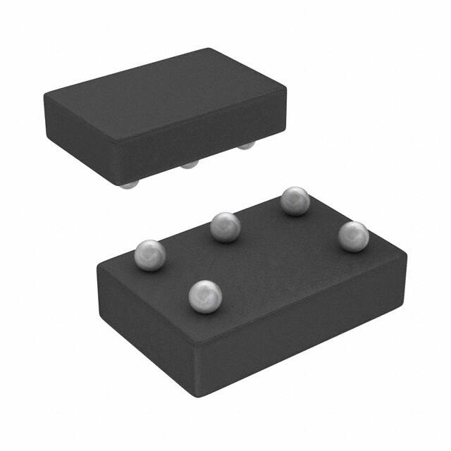
- Package: SOT-23-5
- Essence: Low-Voltage CMOS Logic
- Packaging/Quantity: Tape and Reel, 3000 pieces per reel
Specifications
- Supply Voltage Range: 1.65V to 5.5V
- High-Level Input Voltage: 0.7 x Vcc
- Low-Level Input Voltage: 0.3 x Vcc
- High-Level Output Voltage: 0.9 x Vcc
- Low-Level Output Voltage: 0.1 x Vcc
- Maximum Propagation Delay: 4.3 ns
- Maximum Operating Frequency: 100 MHz
Detailed Pin Configuration
The SN74LVC1G06YZAR has a total of five pins:
- GND (Ground): Connected to the ground reference potential.
- A (Input): Input pin for the logic signal.
- Y (Output): Output pin for the inverted logic signal.
- NC (No Connection): This pin is not connected and should be left unconnected.
- VCC (Power Supply): Connected to the positive power supply voltage.
Functional Features
- Single Inverter Buffer/Driver: The SN74LVC1G06YZAR is designed to invert the logic level of the input signal and provide a buffered output.
- Low-Voltage CMOS Logic: It operates at low voltage levels, making it suitable for battery-powered devices and other low-power applications.
- Fast Propagation Delay: With a maximum propagation delay of 4.3 ns, it ensures quick response times in digital circuits.
- Wide Supply Voltage Range: It can operate within a wide range of supply voltages, from 1.65V to 5.5V.
- High-Speed Operation: The maximum operating frequency of 100 MHz allows for high-speed data processing.
Advantages and Disadvantages
Advantages: - Low power consumption - Small package size - Wide supply voltage range - Fast propagation delay
Disadvantages: - Limited functionality (single inverter buffer/driver) - Not suitable for high-power applications
Working Principles
The SN74LVC1G06YZAR is based on CMOS (Complementary Metal-Oxide-Semiconductor) technology. It consists of a single inverter circuit, which takes the input logic signal and produces an inverted output signal. The CMOS technology ensures low power consumption and allows for operation at low voltage levels.
Detailed Application Field Plans
The SN74LVC1G06YZAR can be used in various applications, including:
- Battery-Powered Devices: Its low power consumption and wide supply voltage range make it ideal for portable electronic devices.
- Communication Systems: It can be used in signal inversion and buffering circuits in communication systems.
- Industrial Control Systems: The fast propagation delay and high-speed operation make it suitable for control and automation applications.
- Automotive Electronics: It can be utilized in automotive electronics for signal conditioning and level shifting.
Detailed and Complete Alternative Models
Some alternative models that offer similar functionality to the SN74LVC1G06YZAR are:
- SN74LVC1G04DBVR: Single Inverter Gate, SOT-23-5 package.
- MC74LCX06DTR2G: Single Inverter Buffer/Driver, SOT-363 package.
- TC7SZU04FUTE85LF: Single Inverter Buffer, SOT-353 package.
These alternatives provide similar logic functions and can be used as replacements depending on specific requirements.
Word count: 452 words
Sebutkan 10 pertanyaan dan jawaban umum terkait penerapan SN74LVC1G06YZAR dalam solusi teknis
Sure! Here are 10 common questions and answers related to the application of SN74LVC1G06YZAR in technical solutions:
Q1: What is SN74LVC1G06YZAR? A1: SN74LVC1G06YZAR is a single inverter gate with open-drain output, which is commonly used in digital logic circuits.
Q2: What is the voltage range supported by SN74LVC1G06YZAR? A2: SN74LVC1G06YZAR supports a voltage range from 1.65V to 5.5V.
Q3: What is the maximum output current of SN74LVC1G06YZAR? A3: The maximum output current of SN74LVC1G06YZAR is typically 32mA.
Q4: Can SN74LVC1G06YZAR be used for level shifting applications? A4: Yes, SN74LVC1G06YZAR can be used for level shifting between different voltage domains.
Q5: Is SN74LVC1G06YZAR suitable for bidirectional communication? A5: No, SN74LVC1G06YZAR is not suitable for bidirectional communication as it only has an open-drain output.
Q6: What is the propagation delay of SN74LVC1G06YZAR? A6: The propagation delay of SN74LVC1G06YZAR is typically around 3.8ns.
Q7: Can SN74LVC1G06YZAR drive capacitive loads? A7: Yes, SN74LVC1G06YZAR can drive small capacitive loads up to a certain limit specified in the datasheet.
Q8: Does SN74LVC1G06YZAR have built-in protection features? A8: Yes, SN74LVC1G06YZAR has built-in protection features like overvoltage and undervoltage lockout.
Q9: Can SN74LVC1G06YZAR be used in high-speed applications? A9: Yes, SN74LVC1G06YZAR can be used in high-speed applications as it has a fast switching speed.
Q10: What is the package type of SN74LVC1G06YZAR? A10: SN74LVC1G06YZAR is available in a small SOT-23 package.