

Lihat spesifikasi untuk detail produk.
SN74LVC16244AZRDR
Basic Information Overview
- Category: Integrated Circuit (IC)
- Use: Buffer/Driver
- Characteristics:
- High-speed CMOS technology
- Low voltage operation
- 16-bit wide buffer/driver
- 3-state outputs
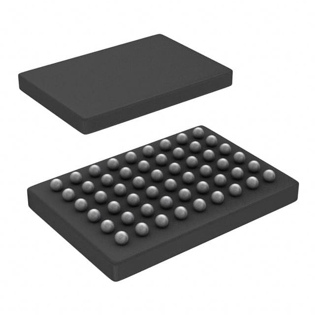
- Package: 48-pin BGA (Ball Grid Array)
- Essence: This IC is designed to provide buffering and driving capabilities for digital signals in various electronic applications.
- Packaging/Quantity: Available in tape and reel packaging, with a quantity of 2500 units per reel.
Specifications
- Supply Voltage Range: 1.65V to 3.6V
- Input Voltage Range: 0V to VCC
- Output Voltage Range: 0V to VCC
- Maximum Operating Frequency: 100 MHz
- Output Drive Capability: ±24 mA
- Propagation Delay: 2.5 ns (typical)
Detailed Pin Configuration
The SN74LVC16244AZRDR has a total of 48 pins. The pin configuration is as follows:
Pin 1:  GND
Pin 2:  A1
Pin 3:  Y1
Pin 4:  A2
Pin 5:  Y2
...
Pin 46: OE#
Pin 47: Y15
Pin 48: VCC
Functional Features
- 16-bit wide buffer/driver with 3-state outputs
- Non-inverting outputs
- Supports bidirectional data flow
- Provides high-speed signal buffering and driving capabilities
- Compatible with various logic families
Advantages
- High-speed operation allows for efficient data transfer
- Low voltage operation reduces power consumption
- 3-state outputs enable bus sharing and multi-master systems
- Wide operating voltage range provides flexibility in different applications
- Compact BGA package offers space-saving benefits
Disadvantages
- Limited output drive capability compared to some other ICs
- Higher cost compared to similar buffer/driver ICs in different packages
- Sensitive to electrostatic discharge (ESD) due to its CMOS technology
Working Principles
The SN74LVC16244AZRDR operates based on high-speed CMOS technology. It receives digital input signals and buffers/drives them to the corresponding outputs. The 3-state outputs allow for bus sharing, where multiple devices can be connected to the same bus without interference. The IC operates within a specified voltage range and provides non-inverting outputs.
Detailed Application Field Plans
The SN74LVC16244AZRDR is widely used in various electronic applications, including: - Data communication systems - Networking equipment - Industrial automation - Automotive electronics - Consumer electronics
In data communication systems, this IC can be used to buffer and drive signals between different components, such as microcontrollers, memory modules, and peripheral devices. In networking equipment, it enables efficient data transfer between network interfaces and processing units. In industrial automation, it facilitates signal transmission between sensors, actuators, and control systems. In automotive electronics, it plays a crucial role in connecting different modules and subsystems. In consumer electronics, it is utilized for signal buffering and driving in devices like smartphones, tablets, and gaming consoles.
Detailed and Complete Alternative Models
Some alternative models that offer similar functionality to the SN74LVC16244AZRDR include: - SN74LVC16245A - SN74LVC16244A - MC74LVX16244 - 74LVC16244ADGGR
These alternatives may differ in terms of package type, pin configuration, or specific characteristics, but they serve the same purpose of buffering and driving digital signals.
Word count: 511 words
Sebutkan 10 pertanyaan dan jawaban umum terkait penerapan SN74LVC16244AZRDR dalam solusi teknis
Sure! Here are 10 common questions and answers related to the application of SN74LVC16244AZRDR in technical solutions:
Q: What is SN74LVC16244AZRDR? A: SN74LVC16244AZRDR is a 16-bit buffer/driver with 3-state outputs, commonly used for signal buffering and level shifting in digital circuits.
Q: What is the voltage range supported by SN74LVC16244AZRDR? A: SN74LVC16244AZRDR supports a wide voltage range from 1.65V to 5.5V, making it compatible with various logic families.
Q: How many output pins does SN74LVC16244AZRDR have? A: SN74LVC16244AZRDR has 16 output pins, each capable of driving up to 32mA of current.
Q: Can SN74LVC16244AZRDR be used for bidirectional communication? A: Yes, SN74LVC16244AZRDR can be used for bidirectional communication as it has 3-state outputs that allow both input and output functionality.
Q: What is the maximum data transfer rate supported by SN74LVC16244AZRDR? A: SN74LVC16244AZRDR can support data transfer rates up to 100MHz, making it suitable for high-speed applications.
Q: Is SN74LVC16244AZRDR tolerant to overvoltage conditions? A: Yes, SN74LVC16244AZRDR has built-in overvoltage tolerance, which protects the device from potential damage due to voltage spikes.
Q: Can SN74LVC16244AZRDR be used in mixed-voltage level shifting applications? A: Yes, SN74LVC16244AZRDR is commonly used for level shifting between different voltage domains, making it suitable for mixed-voltage systems.
Q: Does SN74LVC16244AZRDR have any built-in ESD protection? A: Yes, SN74LVC16244AZRDR has integrated ESD protection on all inputs and outputs, ensuring robustness against electrostatic discharge events.
Q: Can SN74LVC16244AZRDR be cascaded to increase the number of output pins? A: Yes, multiple SN74LVC16244AZRDR devices can be cascaded together to increase the number of output pins in a system.
Q: What is the package type of SN74LVC16244AZRDR? A: SN74LVC16244AZRDR is available in a 48-pin TSSOP (Thin Shrink Small Outline Package) package, which is compact and suitable for space-constrained designs.
Please note that these answers are general and may vary depending on specific application requirements.