

Lihat spesifikasi untuk detail produk.
SN74LVC138AGQNR
Product Overview
- Category: Integrated Circuit (IC)
- Use: Decoder/Demultiplexer
- Characteristics:
- Low-voltage CMOS technology
- High-speed operation
- Low power consumption
- Wide operating voltage range
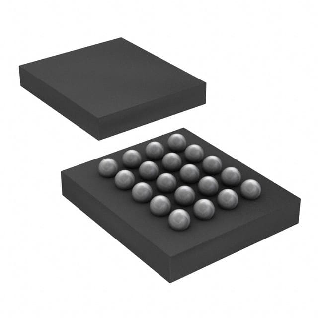
- Package: VQFN-20
- Essence: A decoder/demultiplexer IC that converts a binary input into a corresponding output line.
- Packaging/Quantity: Tape and reel, 2500 units per reel.
Specifications
- Supply Voltage Range: 1.65V to 5.5V
- Input Voltage Range: 0V to VCC
- Output Voltage Range: 0V to VCC
- Operating Temperature Range: -40°C to +85°C
- Maximum Propagation Delay: 6 ns
- Maximum Quiescent Current: 2 μA
- Maximum Output Current: ±24 mA
Detailed Pin Configuration
The SN74LVC138AGQNR has a total of 20 pins, which are assigned as follows:
- GND (Ground)
- Y0 (Output 0)
- Y1 (Output 1)
- Y2 (Output 2)
- G1 (Enable Input 1)
- A0 (Address Input 0)
- A1 (Address Input 1)
- A2 (Address Input 2)
- VCC (Supply Voltage)
- Y3 (Output 3)
- Y4 (Output 4)
- Y5 (Output 5)
- G2A (Enable Input 2A)
- G2B (Enable Input 2B)
- NC (No Connection)
- Y6 (Output 6)
- Y7 (Output 7)
- GND (Ground)
- NC (No Connection)
- NC (No Connection)
Functional Features
- Converts a 3-bit binary input into one of eight corresponding output lines.
- Enables cascading multiple ICs for larger decoding applications.
- Low power consumption makes it suitable for battery-powered devices.
- High-speed operation allows for efficient data processing.
- Wide operating voltage range ensures compatibility with various systems.
Advantages and Disadvantages
Advantages: - Compact VQFN-20 package saves board space. - Low power consumption extends battery life. - High-speed operation enables quick data processing. - Wide operating voltage range provides flexibility in system design.
Disadvantages: - Limited number of output lines (8) compared to other decoder ICs. - Not suitable for high-voltage applications.
Working Principles
The SN74LVC138AGQNR operates based on the principle of binary decoding. The three address inputs (A0, A1, A2) represent a binary code, which is converted into one of the eight output lines (Y0-Y7). The enable inputs (G1, G2A, G2B) control the functioning of the decoder/demultiplexer. When the enable inputs are active, the selected output line reflects the binary input code.
Detailed Application Field Plans
The SN74LVC138AGQNR finds applications in various fields, including:
- Digital electronics: Used in microcontrollers, CPUs, and memory systems for address decoding.
- Communication systems: Employed in multiplexing and demultiplexing circuits.
- Industrial automation: Integrated into control systems for signal routing and selection.
- Automotive electronics: Utilized in vehicle control units for decoding sensor inputs.
- Consumer electronics: Incorporated in remote control systems and audio/video equipment.
Detailed and Complete Alternative Models
- CD74HC138E: High-speed CMOS logic decoder with similar functionality.
- 74HC138N: Standard TTL logic decoder with comparable specifications.
- SN54LS138J: Low-power Schottky TTL decoder/demultiplexer.
These alternative models offer similar decoding capabilities and can be used as substitutes for the SN74LVC138AGQNR in various applications.
Word count: 457 words
Sebutkan 10 pertanyaan dan jawaban umum terkait penerapan SN74LVC138AGQNR dalam solusi teknis
What is the operating voltage range of SN74LVC138AGQNR?
- The operating voltage range of SN74LVC138AGQNR is 1.65V to 5.5V.How many output lines does SN74LVC138AGQNR have?
- SN74LVC138AGQNR has 8 output lines.What is the maximum propagation delay of SN74LVC138AGQNR?
- The maximum propagation delay of SN74LVC138AGQNR is 6.5ns at 3.3V.Can SN74LVC138AGQNR be used in battery-powered applications?
- Yes, SN74LVC138AGQNR can be used in battery-powered applications due to its low operating voltage range.What is the package type of SN74LVC138AGQNR?
- SN74LVC138AGQNR comes in a 16-pin TSSOP package.Is SN74LVC138AGQNR suitable for level shifting applications?
- Yes, SN74LVC138AGQNR is suitable for level shifting applications due to its wide operating voltage range.Does SN74LVC138AGQNR have internal pull-up or pull-down resistors?
- No, SN74LVC138AGQNR does not have internal pull-up or pull-down resistors.Can SN74LVC138AGQNR be used in automotive electronics?
- Yes, SN74LVC138AGQNR is suitable for use in automotive electronics due to its wide operating voltage range and robustness.What is the input capacitance of SN74LVC138AGQNR?
- The input capacitance of SN74LVC138AGQNR is typically 3pF.Is SN74LVC138AGQNR compatible with other 3.3V and 5V logic families?
- Yes, SN74LVC138AGQNR is compatible with a wide range of 3.3V and 5V logic families, making it versatile for various technical solutions.