Lihat spesifikasi untuk detail produk.

SN74LV125ANG4
Product Overview
Category
SN74LV125ANG4 belongs to the category of integrated circuits (ICs).
Use
This product is commonly used as a quad bus buffer gate with 3-state outputs.
Characteristics
- Quad gates: The SN74LV125ANG4 consists of four independent gates, each having a 3-state output.
- Low voltage operation: It operates at a low voltage range of 1.65V to 5.5V, making it suitable for various applications.
- High-speed performance: The SN74LV125ANG4 offers high-speed operation, enabling efficient data transmission.
- 3-state outputs: The 3-state outputs allow multiple devices to share a common bus without interfering with each other.
Package
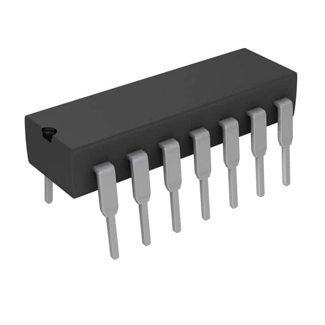
The SN74LV125ANG4 is available in a standard 14-pin DIP (Dual In-line Package) format.
Essence
The essence of SN74LV125ANG4 lies in its ability to provide buffering and signal isolation in digital circuits.
Packaging/Quantity
This product is typically packaged in reels or tubes, with quantities varying based on customer requirements.
Specifications
- Supply Voltage Range: 1.65V to 5.5V
- Input Voltage Range: 0V to VCC
- Output Voltage Range: 0V to VCC
- Operating Temperature Range: -40°C to +85°C
- Maximum Propagation Delay: 6 ns
- Maximum Quiescent Current: 10 µA
Detailed Pin Configuration
The SN74LV125ANG4 has a total of 14 pins, numbered as follows:
- GND (Ground)
- A1 (Input A1)
- Y1 (Output Y1)
- A2 (Input A2)
- Y2 (Output Y2)
- A3 (Input A3)
- Y3 (Output Y3)
- GND (Ground)
- Y4 (Output Y4)
- A4 (Input A4)
- OE (Output Enable)
- VCC (Supply Voltage)
- NC (No Connection)
- GND (Ground)
Functional Features
The SN74LV125ANG4 offers the following functional features:
- Buffering: It provides buffering capability to ensure signal integrity and prevent data loss.
- 3-state outputs: The 3-state outputs allow for bus sharing and isolation, enabling efficient communication between multiple devices.
- High-speed operation: The SN74LV125ANG4 operates at high speeds, facilitating fast data transmission.
Advantages and Disadvantages
Advantages
- Low voltage operation allows for compatibility with a wide range of systems.
- High-speed performance ensures efficient data transfer.
- 3-state outputs enable bus sharing without interference.
Disadvantages
- Limited number of gates per package.
- May require additional components for specific applications.
Working Principles
The SN74LV125ANG4 functions as a quad bus buffer gate with 3-state outputs. It receives input signals from the A1 to A4 pins and buffers them internally. The buffered signals are then available at the corresponding Y1 to Y4 output pins. The OE (Output Enable) pin controls the 3-state outputs, allowing the device to be enabled or disabled as needed.
Detailed Application Field Plans
The SN74LV125ANG4 finds applications in various fields, including:
- Communication Systems: It is used in communication systems to buffer and isolate signals between different components.
- Industrial Automation: The SN74LV125ANG4 facilitates signal transmission and isolation in industrial automation equipment.
- Automotive Electronics: It is employed in automotive electronics for signal buffering and isolation in control modules.
- Consumer Electronics: This product is utilized in consumer electronics devices to ensure reliable signal transmission.
Detailed and Complete Alternative Models
- SN74LV125A: Similar to SN74LV125ANG4, but available in a different package (SOIC-14).
- SN74LVC125A: Offers similar functionality with improved voltage tolerance (1.65V to 3.6V) compared to SN74LV125ANG4.
- SN74HC125: A compatible alternative with higher voltage operation (2V to 6V) and faster propagation delay.
These alternative models provide similar functionality to the SN74LV125ANG4, catering to different application requirements.
Word count: 570 words
Sebutkan 10 pertanyaan dan jawaban umum terkait penerapan SN74LV125ANG4 dalam solusi teknis
Sure! Here are 10 common questions and answers related to the application of SN74LV125ANG4:
Question: What is SN74LV125ANG4?
Answer: SN74LV125ANG4 is a quad bus buffer gate with 3-state outputs, commonly used in digital logic applications.Question: What is the operating voltage range for SN74LV125ANG4?
Answer: The operating voltage range for SN74LV125ANG4 is typically between 1.65V and 5.5V.Question: What is the maximum output current that SN74LV125ANG4 can drive?
Answer: SN74LV125ANG4 can drive up to 12mA of output current per channel.Question: Can SN74LV125ANG4 be used as a level shifter?
Answer: Yes, SN74LV125ANG4 can be used as a level shifter to convert signals between different voltage levels.Question: How many channels does SN74LV125ANG4 have?
Answer: SN74LV125ANG4 has four independent channels, allowing it to buffer or shift signals on multiple lines simultaneously.Question: What is the propagation delay of SN74LV125ANG4?
Answer: The typical propagation delay of SN74LV125ANG4 is around 5.8ns.Question: Can SN74LV125ANG4 be used in high-speed applications?
Answer: Yes, SN74LV125ANG4 is designed for high-speed operation and can be used in applications with fast signal transitions.Question: Does SN74LV125ANG4 have internal pull-up or pull-down resistors?
Answer: No, SN74LV125ANG4 does not have internal pull-up or pull-down resistors. External resistors may be required for certain applications.Question: Can SN74LV125ANG4 be used in both input and output buffer applications?
Answer: Yes, SN74LV125ANG4 can be used as both an input buffer and an output buffer, depending on the application requirements.Question: Is SN74LV125ANG4 available in different package options?
Answer: Yes, SN74LV125ANG4 is available in various package options, such as SOIC, TSSOP, and VQFN, to accommodate different PCB layouts and assembly processes.
Please note that these answers are general and may vary based on specific datasheet specifications and application requirements.

