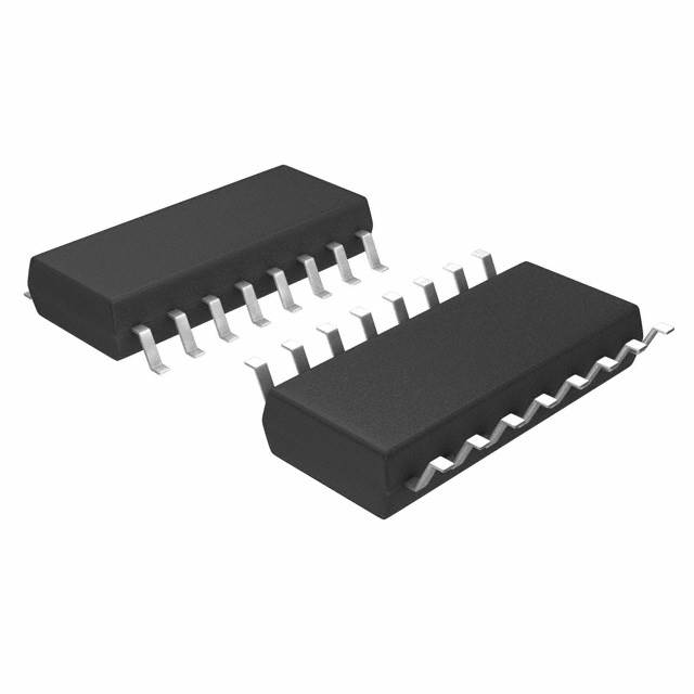
Lihat spesifikasi untuk detail produk.

SN74LS174NSR
Product Overview
Category
SN74LS174NSR belongs to the category of integrated circuits (ICs).
Use
This product is commonly used in electronic devices for data storage and manipulation.
Characteristics
- Low power consumption
- High-speed operation
- Wide operating voltage range
- Compact size
Package
SN74LS174NSR is available in a small outline package (SOIC) with 16 pins.
Essence
The essence of SN74LS174NSR lies in its ability to store and process digital information efficiently.
Packaging/Quantity
This product is typically packaged in reels or tubes, with a quantity of 2500 units per reel.
Specifications
- Supply Voltage: 4.75V to 5.25V
- Operating Temperature Range: -40°C to +85°C
- Logic Family: LS
- Number of Flip-Flops: 6
- Propagation Delay: 15ns (max)
- Output Current: ±8mA
Detailed Pin Configuration
- CLR (Clear)
- D (Data)
- CLK (Clock)
- Q0 (Output 0)
- Q1 (Output 1)
- Q2 (Output 2)
- GND (Ground)
- Q3 (Output 3)
- Q4 (Output 4)
- Q5 (Output 5)
- VCC (Power Supply)
- NC (No Connection)
- NC (No Connection)
- NC (No Connection)
- NC (No Connection)
- NC (No Connection)
Functional Features
- Clear input to reset all flip-flops
- Data input for storing information
- Clock input for synchronizing data transfer
- Six outputs for accessing stored data
- Wide operating voltage range for versatility
Advantages and Disadvantages
Advantages
- Low power consumption makes it suitable for battery-powered devices
- High-speed operation enables quick data processing
- Compact size allows for integration into small electronic systems
- Wide operating voltage range provides flexibility in various applications
Disadvantages
- Limited number of flip-flops may restrict the complexity of data manipulation
- Propagation delay may affect real-time applications with strict timing requirements
Working Principles
SN74LS174NSR operates based on the principles of digital logic. The clock input synchronizes the transfer of data from the D input to the flip-flops. The clear input resets all flip-flops to a known state. The stored information can be accessed through the six output pins.
Detailed Application Field Plans
SN74LS174NSR finds application in various fields, including: 1. Digital communication systems 2. Computer peripherals 3. Industrial automation 4. Consumer electronics 5. Automotive electronics
Detailed and Complete Alternative Models
Some alternative models that serve similar functions to SN74LS174NSR are: 1. 74HC174 2. CD40174 3. MC74HC174 4. DM74LS174
These models offer comparable features and can be used as substitutes depending on specific requirements.
Word count: 410 words
Sebutkan 10 pertanyaan dan jawaban umum terkait penerapan SN74LS174NSR dalam solusi teknis
Sure! Here are 10 common questions and answers related to the application of SN74LS174NSR:
Q: What is SN74LS174NSR? A: SN74LS174NSR is a type of integrated circuit (IC) known as a hex D flip-flop with clear. It is commonly used in digital electronics for storing and manipulating binary data.
Q: What is the purpose of SN74LS174NSR? A: The purpose of SN74LS174NSR is to store and control the flow of digital information in electronic circuits. It can be used for various applications such as data storage, synchronization, and sequential logic.
Q: How many flip-flops are there in SN74LS174NSR? A: SN74LS174NSR contains six individual D flip-flops, each capable of storing one bit of information.
Q: What is the voltage range supported by SN74LS174NSR? A: SN74LS174NSR operates within a voltage range of 4.75V to 5.25V, making it compatible with standard TTL (Transistor-Transistor Logic) levels.
Q: Can SN74LS174NSR handle high-speed data transfers? A: Yes, SN74LS174NSR is designed to operate at high speeds and can handle data transfers up to several megahertz.
Q: How does the clear input work in SN74LS174NSR? A: The clear input allows you to reset all the flip-flops simultaneously. When the clear input is activated, all outputs will be forced to a low state (logic 0).
Q: Can SN74LS174NSR be cascaded to increase the number of flip-flops? A: Yes, SN74LS174NSR can be cascaded by connecting the output of one flip-flop to the input of another. This allows you to increase the number of flip-flops and store more bits of information.
Q: What is the power consumption of SN74LS174NSR? A: The power consumption of SN74LS174NSR is relatively low, typically around a few milliwatts.
Q: Can SN74LS174NSR operate in both rising and falling edge-triggered modes? A: No, SN74LS174NSR is only capable of operating in the rising edge-triggered mode, where data is captured on the rising edge of the clock signal.
Q: Are there any specific precautions to consider when using SN74LS174NSR? A: It is important to ensure that the voltage levels and timing requirements are properly met to avoid any potential issues. Additionally, proper decoupling capacitors should be used to minimize noise and stabilize the power supply.

