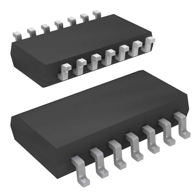
Lihat spesifikasi untuk detail produk.

SN74LS06NSRG4
Product Overview
- Category: Integrated Circuit (IC)
- Use: Inverting Hex Buffer/Driver
- Characteristics:
- Low power Schottky TTL technology
- High-speed operation
- Wide operating voltage range
- Open-collector outputs
- Package: SOIC (Small Outline Integrated Circuit)
- Essence: Hex inverter with open-collector outputs
- Packaging/Quantity: Tape and Reel, 2500 units per reel
Specifications
- Supply Voltage Range: 4.75V to 5.25V
- Input Voltage Range: 0V to Vcc
- Output Voltage Range: 0V to Vcc
- Operating Temperature Range: -40°C to +85°C
- Propagation Delay Time: 9ns (typical)
- Maximum Quiescent Current: 4mA
Detailed Pin Configuration
The SN74LS06NSRG4 has a total of 14 pins. The pin configuration is as follows:
- A1 - Input 1 for the first inverter
- Y1 - Output 1 for the first inverter
- A2 - Input 2 for the second inverter
- Y2 - Output 2 for the second inverter
- A3 - Input 3 for the third inverter
- Y3 - Output 3 for the third inverter
- GND - Ground
- Y4 - Output 4 for the fourth inverter
- A4 - Input 4 for the fourth inverter
- Y5 - Output 5 for the fifth inverter
- A5 - Input 5 for the fifth inverter
- Y6 - Output 6 for the sixth inverter
- A6 - Input 6 for the sixth inverter
- Vcc - Power supply voltage
Functional Features
- Hex inverter with open-collector outputs
- Converts high-level input signals to low-level output signals
- Provides buffering and driving capabilities for digital circuits
- Allows wired-OR connections between multiple devices
- Enables interfacing between different logic families
Advantages and Disadvantages
Advantages: - Low power consumption - High-speed operation - Wide operating voltage range - Open-collector outputs allow flexible circuit design
Disadvantages: - Requires external pull-up resistors for proper operation - Limited output current capability
Working Principles
The SN74LS06NSRG4 is based on the Schottky transistor-transistor logic (TTL) technology. It consists of six independent inverters, each with an open-collector output. When a high-level input signal is applied to an inverter, its output is pulled low due to the open-collector configuration. Conversely, when a low-level input signal is applied, the output remains high impedance.
Detailed Application Field Plans
The SN74LS06NSRG4 can be used in various applications, including: - Logic level shifting - Signal inversion - Bus interfacing - Clock signal conditioning - LED driving - Relay driving - Sensor interfacing
Detailed and Complete Alternative Models
Some alternative models that provide similar functionality to the SN74LS06NSRG4 are: - 74HC06: High-speed CMOS version - CD4069: CMOS version with six inverting gates - MC14069UB: Unbuffered CMOS version with six inverting gates - SN7406: Standard TTL version with six inverting buffers
These alternative models offer compatibility with different logic families and may have variations in speed, power consumption, and voltage ranges.
Word count: 400 words
Sebutkan 10 pertanyaan dan jawaban umum terkait penerapan SN74LS06NSRG4 dalam solusi teknis
Sure! Here are 10 common questions and answers related to the application of SN74LS06NSRG4 in technical solutions:
Q: What is SN74LS06NSRG4? A: SN74LS06NSRG4 is a hex inverter gate IC (integrated circuit) that is commonly used in digital logic circuits.
Q: What is the purpose of SN74LS06NSRG4? A: The purpose of SN74LS06NSRG4 is to invert the input signal, i.e., it converts a high-level input to a low-level output and vice versa.
Q: What voltage levels does SN74LS06NSRG4 support? A: SN74LS06NSRG4 supports a wide range of voltage levels, typically from 2V to 6V.
Q: How many inverters are there in SN74LS06NSRG4? A: SN74LS06NSRG4 consists of six independent inverters in a single package.
Q: Can SN74LS06NSRG4 be used in both TTL and CMOS logic circuits? A: Yes, SN74LS06NSRG4 can be used in both TTL (Transistor-Transistor Logic) and CMOS (Complementary Metal-Oxide-Semiconductor) logic circuits.
Q: What is the maximum frequency at which SN74LS06NSRG4 can operate? A: SN74LS06NSRG4 can typically operate at frequencies up to 30 MHz.
Q: Is SN74LS06NSRG4 suitable for driving capacitive loads? A: No, SN74LS06NSRG4 is not recommended for driving capacitive loads directly. It is better to use a buffer or driver IC for that purpose.
Q: Can SN74LS06NSRG4 be used in high-noise environments? A: SN74LS06NSRG4 is not specifically designed for high-noise environments, so additional noise filtering may be required.
Q: What is the power supply voltage range for SN74LS06NSRG4? A: The power supply voltage range for SN74LS06NSRG4 is typically between 4.75V and 5.25V.
Q: Are there any specific precautions to consider when using SN74LS06NSRG4? A: It is important to avoid exceeding the maximum ratings specified in the datasheet, such as voltage and temperature limits, to ensure proper operation and reliability of SN74LS06NSRG4.
Please note that these answers are general and may vary depending on the specific application and requirements. Always refer to the datasheet and consult with a technical expert for accurate information.

