

Lihat spesifikasi untuk detail produk.
SN74ALVCH162832GR
Product Overview
- Category: Integrated Circuit (IC)
- Use: Logic Level Translator
- Characteristics:
- High-speed, low-power CMOS technology
- Wide voltage translation range
- Bidirectional voltage translation
- Supports mixed-mode signal operation
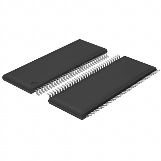
- Package: 56-pin TSSOP (Thin Shrink Small Outline Package)
- Essence: This IC is designed to provide voltage level translation between different logic families.
- Packaging/Quantity: Available in reels of 2500 units.
Specifications
- Supply Voltage Range: 1.2V to 3.6V
- Input Voltage Range (VREF): 0V to VCC
- Output Voltage Range (A/B Ports): 0V to VCC
- Operating Temperature Range: -40°C to +85°C
- Propagation Delay: 2.5ns (typical)
- Maximum Frequency: 400MHz
Detailed Pin Configuration
The SN74ALVCH162832GR has a total of 56 pins. Here is the detailed pin configuration:
- OEAB
- A1
- A2
- A3
- A4
- A5
- A6
- A7
- A8
- GND
- B1
- B2
- B3
- B4
- B5
- B6
- B7
- B8
- VCC
- OEA
- A9
- A10
- A11
- A12
- A13
- A14
- A15
- A16
- GND
- B9
- B10
- B11
- B12
- B13
- B14
- B15
- B16
- VCC
- OEB
- A17
- A18
- A19
- A20
- A21
- A22
- A23
- A24
- GND
- B17
- B18
- B19
- B20
- B21
- B22
- B23
- B24
Functional Features
- Bidirectional voltage translation between two logic families.
- Supports mixed-mode signal operation, allowing different voltage levels on each side.
- High-speed operation with low propagation delay.
- Low power consumption due to CMOS technology.
Advantages and Disadvantages
Advantages: - Wide voltage translation range allows compatibility between various logic families. - Supports bidirectional communication, reducing the need for additional components. - High-speed operation enables efficient data transfer. - Low power consumption helps in energy-efficient designs.
Disadvantages: - Limited to a specific package type (TSSOP). - May require additional circuitry for level shifting in certain applications.
Working Principles
The SN74ALVCH162832GR utilizes CMOS technology to achieve voltage level translation. It consists of multiple transistors and logic gates that enable bidirectional signal conversion between two logic families. The input signals are detected and processed by the internal circuitry, which then generates the corresponding output signals at the desired voltage levels.
Detailed Application Field Plans
The SN74ALVCH162832GR is commonly used in various applications, including:
- Microcontroller interfacing: It facilitates communication between microcontrollers operating at different voltage levels.
- Memory systems: Enables data transfer between memory modules with different logic families.
- Communication interfaces: Provides voltage level translation for UART, SPI, I2C, and other communication protocols.
- Industrial automation: Used in control systems to interface between different logic families.
Detailed and Complete Alternative Models
- SN74ALVC164245: 16-bit voltage level translator with 3-state outputs.
- SN74LVC1T45: Single-bit bidirectional voltage level translator.
- SN74AVC4T774: Quad-bit voltage level translator with configurable voltage levels.
- SN74LVCH16244A: 16-bit buffer/driver with voltage level translation capabilities.
These alternative models offer similar functionality and can be considered as alternatives to the SN74ALVCH162832GR based on specific application requirements.
Word count: 534 words
Sebutkan 10 pertanyaan dan jawaban umum terkait penerapan SN74ALVCH162832GR dalam solusi teknis
Sure! Here are 10 common questions and answers related to the application of SN74ALVCH162832GR:
Q: What is SN74ALVCH162832GR? A: SN74ALVCH162832GR is a 18-bit universal bus driver with 3-state outputs, designed for low-voltage (1.65V to 3.6V) applications.
Q: What is the maximum operating frequency of SN74ALVCH162832GR? A: The maximum operating frequency of SN74ALVCH162832GR is typically around 400 MHz.
Q: Can SN74ALVCH162832GR be used in both input and output applications? A: Yes, SN74ALVCH162832GR can be used as both an input buffer and an output driver.
Q: What is the output drive strength of SN74ALVCH162832GR? A: SN74ALVCH162832GR has a typical output drive strength of ±24 mA.
Q: Does SN74ALVCH162832GR support hot insertion? A: Yes, SN74ALVCH162832GR supports hot insertion, which means it can be inserted or removed from a live circuit without causing damage.
Q: Can SN74ALVCH162832GR be used in mixed-voltage level translation applications? A: Yes, SN74ALVCH162832GR is suitable for mixed-voltage level translation between different voltage domains.
Q: What is the power supply voltage range for SN74ALVCH162832GR? A: SN74ALVCH162832GR operates within a power supply voltage range of 1.65V to 3.6V.
Q: Does SN74ALVCH162832GR have built-in ESD protection? A: Yes, SN74ALVCH162832GR has built-in ESD protection to safeguard against electrostatic discharge.
Q: Can SN74ALVCH162832GR be used in high-speed data transmission applications? A: Yes, SN74ALVCH162832GR is suitable for high-speed data transmission due to its low propagation delay and fast switching characteristics.
Q: What package options are available for SN74ALVCH162832GR? A: SN74ALVCH162832GR is available in various package options, such as TSSOP, TVSOP, and VFBGA, to accommodate different PCB layouts and assembly requirements.
Please note that the answers provided here are general and may vary depending on specific datasheet specifications and application requirements.