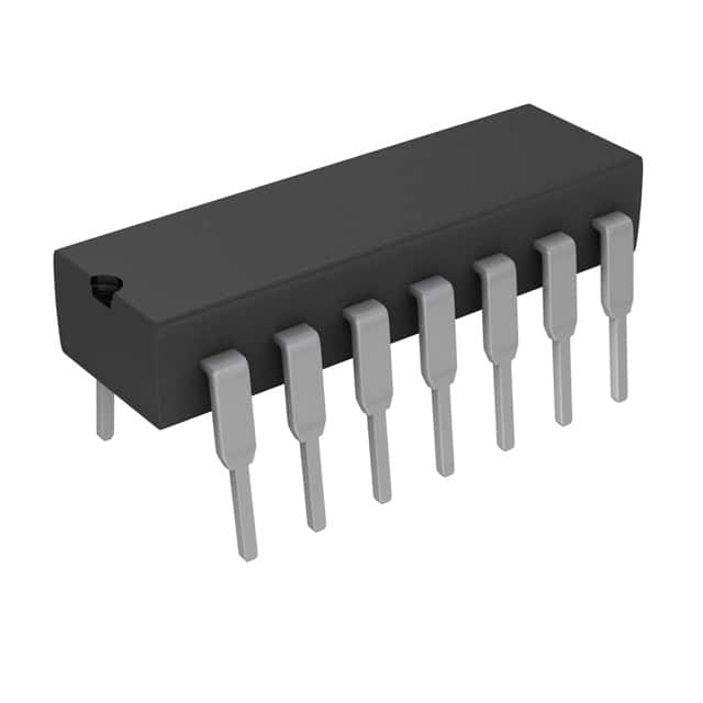
Lihat spesifikasi untuk detail produk.

SN74AHCT04N
Product Overview
- Category: Integrated Circuit
- Use: Inverter
- Characteristics: High-speed, low-power consumption
- Package: DIP (Dual Inline Package)
- Essence: Hex inverter gate
- Packaging/Quantity: Tube/25 pieces
Specifications
- Supply Voltage Range: 2V to 5.5V
- Input Voltage Range: 0V to VCC
- Output Voltage Range: 0V to VCC
- Maximum Operating Frequency: 50 MHz
- Propagation Delay Time: 9 ns (typical)
- Operating Temperature Range: -40°C to +85°C
Detailed Pin Configuration
The SN74AHCT04N has a total of 14 pins, which are numbered as follows:
- A1 (Input)
- Y1 (Output)
- A2 (Input)
- Y2 (Output)
- A3 (Input)
- Y3 (Output)
- GND (Ground)
- Y4 (Output)
- A4 (Input)
- Y5 (Output)
- A5 (Input)
- Y6 (Output)
- VCC (Power Supply)
- A6 (Input)
Functional Features
- Hex Inverter: The SN74AHCT04N consists of six independent inverters, each capable of converting a logic level from high to low or vice versa.
- High-Speed Operation: With a maximum operating frequency of 50 MHz, the SN74AHCT04N ensures fast signal processing.
- Low Power Consumption: This integrated circuit is designed to consume minimal power, making it suitable for battery-powered devices.
Advantages and Disadvantages
Advantages: - High-speed operation allows for quick signal processing. - Low power consumption extends battery life in portable devices. - Hex inverter configuration provides flexibility in logic circuit design.
Disadvantages: - Limited voltage range (2V to 5.5V) may not be suitable for all applications. - Propagation delay time of 9 ns may introduce timing issues in certain high-speed applications.
Working Principles
The SN74AHCT04N operates based on the principles of digital logic. Each inverter within the IC takes an input signal and produces the logical complement of that signal at its output. The hex inverter gate configuration allows for versatile logic circuit design by providing six independent inverters in a single package.
Detailed Application Field Plans
The SN74AHCT04N is widely used in various digital systems and electronic devices, including but not limited to:
- Microcontrollers: Used for signal inversion and level shifting between different logic families.
- Communication Systems: Employed in data transmission circuits to convert logic levels.
- Computer Peripherals: Integrated into interface circuits for signal conversion and buffering.
- Consumer Electronics: Utilized in audio/video equipment, gaming consoles, and remote controls for signal processing.
Detailed and Complete Alternative Models
- SN74AHC04: Similar to SN74AHCT04N, but operates at a wider voltage range of 2V to 5.5V.
- CD4069UB: Hex inverter IC with a broader operating temperature range (-55°C to +125°C).
- MC74HC04: High-speed CMOS inverter with a maximum operating frequency of 74 MHz.
These alternative models offer similar functionality to the SN74AHCT04N and can be considered as substitutes depending on specific requirements.
Word count: 408 words
Sebutkan 10 pertanyaan dan jawaban umum terkait penerapan SN74AHCT04N dalam solusi teknis
Sure! Here are 10 common questions and answers related to the application of SN74AHCT04N:
Q: What is SN74AHCT04N? A: SN74AHCT04N is a hex inverter gate IC, which means it has six independent inverters that can be used for logic level conversion or signal inversion.
Q: What is the voltage supply range for SN74AHCT04N? A: SN74AHCT04N operates with a voltage supply range of 2V to 5.5V.
Q: Can SN74AHCT04N be used for level shifting between different voltage domains? A: Yes, SN74AHCT04N can be used for level shifting as it supports both TTL (5V) and CMOS (3.3V) logic levels.
Q: How much current can SN74AHCT04N source or sink? A: SN74AHCT04N can source or sink up to 8mA of current per output pin.
Q: Is SN74AHCT04N suitable for high-speed applications? A: No, SN74AHCT04N is not designed for high-speed applications. It has a typical propagation delay of 9ns.
Q: Can I use SN74AHCT04N in an automotive application? A: Yes, SN74AHCT04N is suitable for automotive applications as it can operate within the specified temperature range (-40°C to 125°C).
Q: Does SN74AHCT04N have any built-in protection features? A: No, SN74AHCT04N does not have built-in protection features like overvoltage or ESD protection. External protection may be required.
Q: Can I use SN74AHCT04N in a battery-powered application? A: Yes, SN74AHCT04N can be used in battery-powered applications as it operates within a wide voltage supply range and has low power consumption.
Q: What is the pin configuration of SN74AHCT04N? A: SN74AHCT04N has 14 pins, with each inverter having an input (A) and an output (Y).
Q: Are there any alternative ICs to SN74AHCT04N? A: Yes, there are alternative hex inverter gate ICs available from different manufacturers, such as CD74HC04, 74HCT04, or MC74ACT04.
Please note that these answers are general and may vary depending on specific application requirements.

