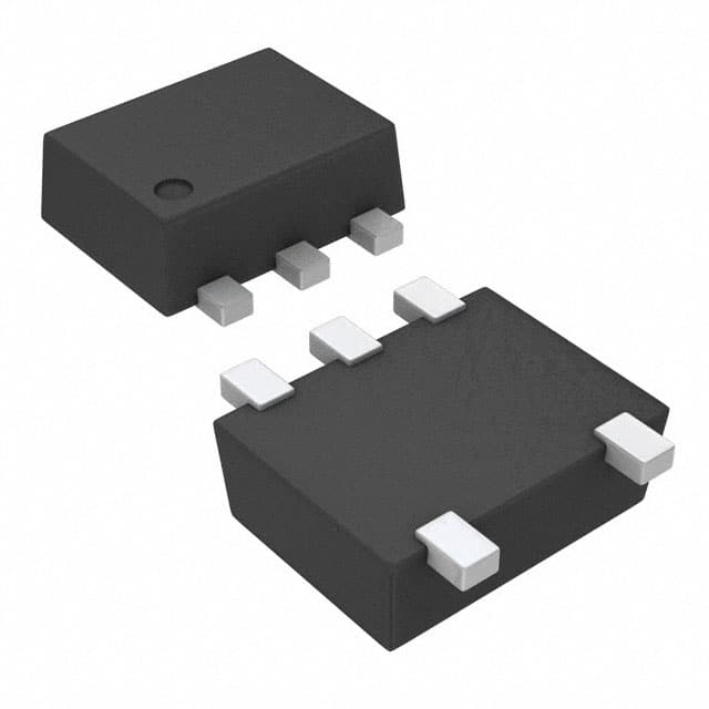
Lihat spesifikasi untuk detail produk.

SN74AHC1G08DRLR
Product Overview
- Category: Integrated Circuit
- Use: Logic Gate
- Characteristics: Single 2-Input AND Gate
- Package: SOT-353 (SC-88A)
- Essence: High-Speed CMOS Technology
- Packaging/Quantity: Tape and Reel, 3000 pieces per reel
Specifications
- Supply Voltage Range: 2 V to 5.5 V
- Input Voltage Range: 0 V to VCC
- Output Voltage Range: 0 V to VCC
- Operating Temperature Range: -40°C to +125°C
- Propagation Delay: 4.5 ns (typical)
- Maximum Quiescent Current: 1 µA at 5.5 V
- Maximum Output Current: ±8 mA
Detailed Pin Configuration
The SN74AHC1G08DRLR has the following pin configuration:
____
   A --|    |-- VCC
   B --|    |-- Y
 GND --|____|-- NC
Functional Features
- Single 2-input AND gate functionality
- High-speed operation using advanced CMOS technology
- Wide supply voltage range for compatibility with various systems
- Low power consumption with maximum quiescent current of 1 µA
- Small package size for space-constrained applications
Advantages and Disadvantages
Advantages: - High-speed operation allows for efficient logic processing - Wide supply voltage range enables compatibility with different systems - Low power consumption reduces energy usage - Small package size saves space in electronic designs
Disadvantages: - Limited to 2-input AND gate functionality - May not be suitable for complex logic operations requiring multiple gates
Working Principles
The SN74AHC1G08DRLR is a single 2-input AND gate that operates using high-speed CMOS technology. It takes two input signals, A and B, and produces an output signal, Y, based on the logical AND operation between the inputs. The gate operates within a wide supply voltage range of 2 V to 5.5 V and consumes low power with a maximum quiescent current of 1 µA.
Detailed Application Field Plans
The SN74AHC1G08DRLR can be used in various applications that require logic operations. Some potential application fields include:
Digital Logic Systems: The AND gate is a fundamental building block in digital logic systems. The SN74AHC1G08DRLR can be used to implement logical functions in microcontrollers, processors, and other digital circuits.
Communication Systems: The gate can be utilized in communication systems for signal processing, data routing, and error detection. It helps in controlling the flow of information and ensuring accurate transmission.
Industrial Automation: In industrial automation, the AND gate can be employed to control sensors, actuators, and other devices. It enables logical decision-making based on multiple input conditions.
Automotive Electronics: The gate finds applications in automotive electronics for functions like engine control, safety systems, and infotainment. It assists in processing signals and making critical decisions.
Detailed and Complete Alternative Models
Some alternative models that offer similar functionality to the SN74AHC1G08DRLR are:
- 74HC08: This is a popular alternative from the 74HC series, offering a 2-input AND gate in various package options.
- CD4081: A CMOS-based quad 2-input AND gate that provides multiple gates in a single package.
- MC14008B: A 4-bit AND gate IC with four independent 2-input AND gates, suitable for more complex logic operations.
These alternative models can be considered based on specific requirements and availability.
Word count: 439 words
Sebutkan 10 pertanyaan dan jawaban umum terkait penerapan SN74AHC1G08DRLR dalam solusi teknis
Sure! Here are 10 common questions and answers related to the application of SN74AHC1G08DRLR in technical solutions:
Q1: What is SN74AHC1G08DRLR? A1: SN74AHC1G08DRLR is a single 2-input AND gate IC (integrated circuit) from Texas Instruments.
Q2: What is the voltage supply range for SN74AHC1G08DRLR? A2: The voltage supply range for SN74AHC1G08DRLR is typically between 2 V and 5.5 V.
Q3: What is the maximum output current of SN74AHC1G08DRLR? A3: The maximum output current of SN74AHC1G08DRLR is 8 mA.
Q4: Can SN74AHC1G08DRLR be used as a level shifter? A4: Yes, SN74AHC1G08DRLR can be used as a level shifter to convert signals between different voltage levels.
Q5: What is the propagation delay of SN74AHC1G08DRLR? A5: The propagation delay of SN74AHC1G08DRLR is typically around 4 ns.
Q6: Can SN74AHC1G08DRLR be used in high-speed applications? A6: Yes, SN74AHC1G08DRLR is suitable for high-speed applications due to its low propagation delay.
Q7: Is SN74AHC1G08DRLR compatible with other logic families? A7: Yes, SN74AHC1G08DRLR is compatible with other CMOS logic families.
Q8: Can SN74AHC1G08DRLR be used in battery-powered devices? A8: Yes, SN74AHC1G08DRLR can be used in battery-powered devices as it operates at low voltage levels.
Q9: What is the package type of SN74AHC1G08DRLR? A9: SN74AHC1G08DRLR comes in a small SOT-23-5 package.
Q10: Can SN74AHC1G08DRLR be used in automotive applications? A10: Yes, SN74AHC1G08DRLR is suitable for automotive applications as it meets the required standards and specifications.
Please note that these answers are general and may vary depending on specific application requirements.

