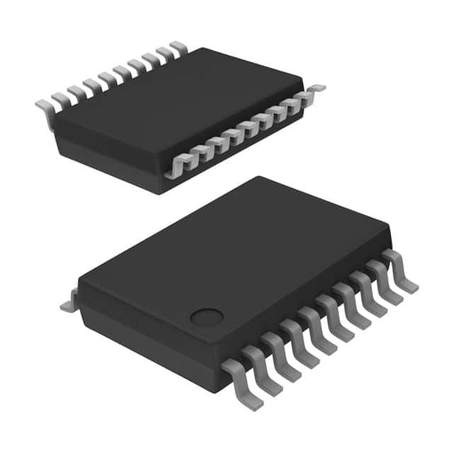
Lihat spesifikasi untuk detail produk.

SN74ACT374DBRE4
Product Overview
- Category: Integrated Circuit (IC)
- Use: Flip-Flop
- Characteristics: High-speed, low-power, octal D-type flip-flop
- Package: SSOP (Shrink Small Outline Package)
- Essence: A versatile and efficient flip-flop IC used in various digital applications
- Packaging/Quantity: Tape and Reel, 2500 units per reel
Specifications
- Logic Family: ACT
- Number of Flip-Flops: 8
- Input Voltage Range: 2V to 6V
- Propagation Delay Time: 5.5ns (typical)
- Output Drive Capability: ±24mA
- Operating Temperature Range: -40°C to +85°C
Detailed Pin Configuration
The SN74ACT374DBRE4 has a total of 20 pins. The pin configuration is as follows:
- Clear (CLR)
- Data Inputs (D0-D7)
- Clock (CLK)
- Output Enable (OE)
- Outputs (Q0-Q7)
- Ground (GND)
- VCC (Power Supply)
Functional Features
- Octal D-type flip-flop with asynchronous clear functionality
- High-speed operation suitable for time-critical applications
- Low power consumption for energy-efficient designs
- Wide input voltage range allows compatibility with various systems
- Output drive capability enables direct connection to other components
Advantages and Disadvantages
Advantages: - High-speed operation improves overall system performance - Low power consumption reduces energy costs - Versatile design allows for a wide range of applications - Compact SSOP package saves board space
Disadvantages: - Limited output drive capability may require additional buffering for certain applications - Not suitable for high-voltage or high-current applications
Working Principles
The SN74ACT374DBRE4 is a positive-edge-triggered flip-flop. It stores and transfers data based on the rising edge of the clock signal. The asynchronous clear functionality allows for immediate resetting of all flip-flops when the clear input is activated. This IC operates within a specified voltage range and provides stable outputs based on the input data.
Detailed Application Field Plans
The SN74ACT374DBRE4 is widely used in various digital systems, including but not limited to: - Microcontrollers - Data storage devices - Communication equipment - Industrial automation systems - Consumer electronics
Detailed and Complete Alternative Models
- SN74ACT374D: Similar specifications and features, available in different package options.
- 74ACT374: Equivalent functionality from other manufacturers, may have slight variations in specifications.
- CD74ACT374: Comparable octal D-type flip-flop IC with similar characteristics.
These alternative models provide similar functionality and can be considered as replacements depending on specific requirements.
In conclusion, the SN74ACT374DBRE4 is a versatile and efficient octal D-type flip-flop IC. Its high-speed operation, low power consumption, and compact package make it suitable for a wide range of digital applications. While it has certain limitations in terms of output drive capability, it offers reliable performance and is widely used in various industries.
Sebutkan 10 pertanyaan dan jawaban umum terkait penerapan SN74ACT374DBRE4 dalam solusi teknis
Sure! Here are 10 common questions and answers related to the application of SN74ACT374DBRE4 in technical solutions:
Q: What is SN74ACT374DBRE4? A: SN74ACT374DBRE4 is a type of octal D-type flip-flop with 3-state outputs, commonly used in digital circuits.
Q: What is the operating voltage range for SN74ACT374DBRE4? A: The operating voltage range for SN74ACT374DBRE4 is typically between 4.5V and 5.5V.
Q: How many flip-flops are there in SN74ACT374DBRE4? A: SN74ACT374DBRE4 consists of 8 individual D-type flip-flops.
Q: What is the maximum clock frequency supported by SN74ACT374DBRE4? A: SN74ACT374DBRE4 can support clock frequencies up to 100 MHz.
Q: Can SN74ACT374DBRE4 be used for level shifting applications? A: Yes, SN74ACT374DBRE4 can be used for level shifting as it supports both TTL and CMOS logic levels.
Q: What is the output drive capability of SN74ACT374DBRE4? A: SN74ACT374DBRE4 has a typical output drive capability of ±24 mA.
Q: Is SN74ACT374DBRE4 compatible with other logic families? A: Yes, SN74ACT374DBRE4 is compatible with a wide range of logic families including TTL, CMOS, and LVTTL.
Q: Can SN74ACT374DBRE4 be used in high-speed data transfer applications? A: Yes, SN74ACT374DBRE4 is suitable for high-speed data transfer applications due to its fast propagation delay.
Q: Does SN74ACT374DBRE4 have any built-in protection features? A: Yes, SN74ACT374DBRE4 has built-in ESD (Electrostatic Discharge) protection to prevent damage from static electricity.
Q: What is the package type of SN74ACT374DBRE4? A: SN74ACT374DBRE4 is available in a small-outline integrated circuit (SOIC) package with 20 pins.
Please note that these answers are general and may vary depending on specific datasheet specifications and application requirements.

