Lihat spesifikasi untuk detail produk.

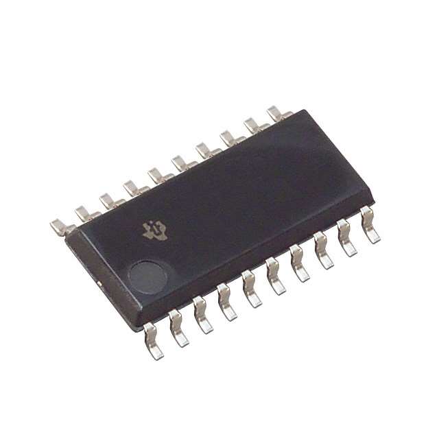
SN74AC374NSRE4
Product Overview
- Category: Integrated Circuit (IC)
- Use: Flip-Flop
- Characteristics: High-speed, low-power, octal D-type flip-flop
- Package: 20-pin small-outline integrated circuit (SOIC)
- Essence: Sequential logic device for storing and transferring data
- Packaging/Quantity: Tape and reel, 2500 units per reel
Specifications
- Supply Voltage Range: 2 V to 6 V
- High-Level Input Voltage: 2 V to VCC
- Low-Level Input Voltage: GND to 0.8 V
- High-Level Output Voltage: VCC - 0.5 V
- Low-Level Output Voltage: 0.5 V
- Maximum Operating Frequency: 125 MHz
- Propagation Delay Time: 3.5 ns
- Operating Temperature Range: -40°C to +85°C
Detailed Pin Configuration
- Clock (CLK)
- Data Enable (EN)
- Data Inputs (D0-D7)
- Output Enable (OE)
- Outputs (Q0-Q7)
- Ground (GND)
- Supply Voltage (VCC)
Functional Features
- Octal D-type flip-flop with 3-state outputs
- Positive-edge triggered clock input
- Asynchronous clear input for resetting the flip-flop
- 3-state outputs allow multiple devices to be connected in parallel
- High-speed operation with low power consumption
- Schmitt-trigger inputs for noise immunity
Advantages
- High-speed operation allows for efficient data transfer
- Low power consumption reduces energy usage
- 3-state outputs enable easy interfacing with other devices
- Schmitt-trigger inputs provide robustness against noise
Disadvantages
- Limited operating frequency compared to some newer flip-flop designs
- May not be suitable for applications requiring very high-speed data processing
Working Principles
The SN74AC374NSRE4 is a positive-edge triggered octal D-type flip-flop. It stores and transfers data based on the rising edge of the clock input (CLK). The data inputs (D0-D7) are latched into the flip-flop when the clock signal transitions from low to high. The output enable (OE) pin controls the 3-state outputs (Q0-Q7), allowing them to be either active or in a high-impedance state. The asynchronous clear input (EN) resets the flip-flop, forcing all outputs to a low state.
Detailed Application Field Plans
The SN74AC374NSRE4 is widely used in various digital systems where sequential logic is required. Some common application fields include:
- Microprocessors and microcontrollers
- Data storage systems
- Communication devices
- Industrial automation
- Automotive electronics
- Consumer electronics
Detailed and Complete Alternative Models
- SN74AC574: Octal D-type flip-flop with inverted outputs
- SN74ACT374: Octal D-type flip-flop with TTL-compatible inputs
- SN74HC374: Octal D-type flip-flop with CMOS-compatible inputs
- SN74HCT374: Octal D-type flip-flop with CMOS/TTL-compatible inputs
- SN74LV374A: Octal D-type flip-flop with low-voltage operation
These alternative models offer similar functionality but may have different characteristics, package options, or voltage requirements.
Word count: 335 words
Sebutkan 10 pertanyaan dan jawaban umum terkait penerapan SN74AC374NSRE4 dalam solusi teknis
Sure! Here are 10 common questions and answers related to the application of SN74AC374NSRE4 in technical solutions:
Q: What is SN74AC374NSRE4? A: SN74AC374NSRE4 is a type of integrated circuit (IC) commonly used as an octal D-type flip-flop with 3-state outputs.
Q: What are the key features of SN74AC374NSRE4? A: Some key features include high-speed operation, low power consumption, 3-state outputs, and compatibility with various logic families.
Q: How can SN74AC374NSRE4 be used in technical solutions? A: It can be used for data storage, signal buffering, address latching, and other applications that require sequential control or data manipulation.
Q: What is the maximum operating frequency of SN74AC374NSRE4? A: The maximum operating frequency is typically specified by the manufacturer and can vary, but it is generally in the range of several hundred megahertz.
Q: What is the voltage supply range for SN74AC374NSRE4? A: The voltage supply range is typically between 2V and 6V, allowing it to be used with both TTL and CMOS logic levels.
Q: Can SN74AC374NSRE4 handle bidirectional data flow? A: No, SN74AC374NSRE4 is a unidirectional device and can only handle data flow in one direction.
Q: Does SN74AC374NSRE4 have any built-in protection features? A: Yes, it has built-in diode clamps on the inputs to protect against electrostatic discharge (ESD) and other transient events.
Q: What is the typical output current capability of SN74AC374NSRE4? A: The typical output current capability is around 24mA, allowing it to drive standard TTL or CMOS loads.
Q: Can SN74AC374NSRE4 be cascaded to increase the number of flip-flops? A: Yes, multiple SN74AC374NSRE4 ICs can be cascaded together to create larger storage registers or shift registers.
Q: Are there any specific layout considerations for using SN74AC374NSRE4? A: Yes, it is recommended to follow proper decoupling and grounding techniques, minimize trace lengths, and avoid signal integrity issues for optimal performance.
Please note that these answers are general and may vary depending on the specific datasheet and manufacturer's recommendations for SN74AC374NSRE4.

