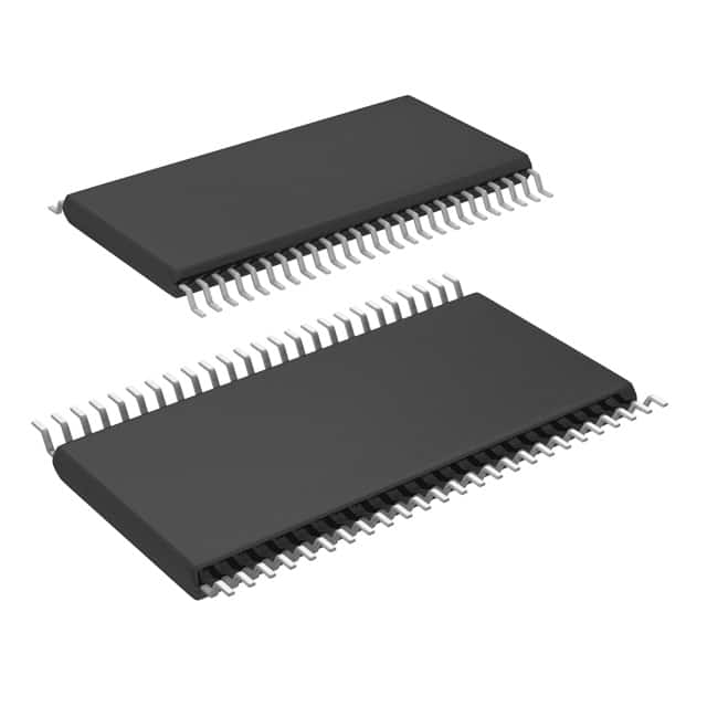
Lihat spesifikasi untuk detail produk.

SN74ABT16244ADGGR
Product Overview
- Category: Integrated Circuit (IC)
- Use: Buffer/Driver
- Characteristics: High-speed, non-inverting, 16-bit bus transceiver
- Package: TSSOP-48
- Essence: Transmits and receives data between two bidirectional buses
- Packaging/Quantity: Tape and Reel, 2500 units per reel
Specifications
- Logic Family: ABT
- Number of Bits: 16
- Input Voltage Range: 2V to 5.5V
- Output Voltage Range: 0V to VCC
- Propagation Delay Time: 3.8ns (typical)
- Operating Temperature Range: -40°C to +85°C
Detailed Pin Configuration
The SN74ABT16244ADGGR has a total of 48 pins. The pin configuration is as follows:
- OE (Output Enable) 1
- A1 (Data Bus A) 1
- A2 (Data Bus A) 2
- GND (Ground)
- B1 (Data Bus B) 1
- B2 (Data Bus B) 2
- Y1 (Data Bus Y) 1
- Y2 (Data Bus Y) 2
- VCC (Power Supply)
- GND (Ground)
- Y3 (Data Bus Y) 3
- Y4 (Data Bus Y) 4
- B3 (Data Bus B) 3
- B4 (Data Bus B) 4
- A3 (Data Bus A) 3
- A4 (Data Bus A) 4
- OE (Output Enable) 2
- GND (Ground)
- A5 (Data Bus A) 5
- A6 (Data Bus A) 6
- B5 (Data Bus B) 5
- B6 (Data Bus B) 6
- Y5 (Data Bus Y) 5
- Y6 (Data Bus Y) 6
- VCC (Power Supply)
- GND (Ground)
- Y7 (Data Bus Y) 7
- Y8 (Data Bus Y) 8
- B7 (Data Bus B) 7
- B8 (Data Bus B) 8
- A7 (Data Bus A) 7
- A8 (Data Bus A) 8
- OE (Output Enable) 3
- GND (Ground)
- A9 (Data Bus A) 9
- A10 (Data Bus A) 10
- B9 (Data Bus B) 9
- B10 (Data Bus B) 10
- Y9 (Data Bus Y) 9
- Y10 (Data Bus Y) 10
- VCC (Power Supply)
- GND (Ground)
- Y11 (Data Bus Y) 11
- Y12 (Data Bus Y) 12
- B11 (Data Bus B) 11
- B12 (Data Bus B) 12
- A11 (Data Bus A) 11
- A12 (Data Bus A) 12
Functional Features
- Bidirectional data flow between two buses
- Non-inverting logic
- High-speed operation
- Output enable control for bus isolation
Advantages and Disadvantages
Advantages: - High-speed operation allows for efficient data transmission - Non-inverting logic simplifies circuit design - Output enable control provides flexibility in bus isolation
Disadvantages: - Limited number of bits (16) may not be suitable for larger data transfers - Requires external power supply and ground connections
Working Principles
The SN74ABT16244ADGGR is a 16-bit bus transceiver that enables bidirectional data transfer between two buses. It operates using non-inverting logic, meaning the input signal is reproduced at the output without any inversion. The transceiver has an output enable control pin that allows for bus isolation when needed.
When the output enable pin is active, the transceiver is enabled, and data can flow freely between the input and output buses. When the output enable pin is inactive, the transceiver isolates the input and output buses, preventing any data transfer.
Detailed Application Field Plans
The SN74ABT16244ADGGR is commonly used in various applications where bidirectional data transfer is required. Some of the typical application fields include:
- Data communication systems
- Memory interfaces
- Microprocessor systems
- Industrial automation
Sebutkan 10 pertanyaan dan jawaban umum terkait penerapan SN74ABT16244ADGGR dalam solusi teknis
Sure! Here are 10 common questions and answers related to the application of SN74ABT16244ADGGR:
Question: What is the SN74ABT16244ADGGR?
Answer: The SN74ABT16244ADGGR is a 16-bit buffer/driver with 3-state outputs, commonly used in digital systems.Question: What is the operating voltage range of SN74ABT16244ADGGR?
Answer: The operating voltage range is typically between 4.5V and 5.5V.Question: What is the maximum output current of SN74ABT16244ADGGR?
Answer: The maximum output current is typically 32mA.Question: Can I use SN74ABT16244ADGGR for level shifting between different voltage domains?
Answer: Yes, SN74ABT16244ADGGR can be used for level shifting as it supports bidirectional voltage translation.Question: What is the propagation delay of SN74ABT16244ADGGR?
Answer: The propagation delay is typically around 4.5ns.Question: How many 3-state outputs does SN74ABT16244ADGGR have?
Answer: SN74ABT16244ADGGR has 16 3-state outputs.Question: Can I connect multiple SN74ABT16244ADGGR devices together?
Answer: Yes, you can connect multiple SN74ABT16244ADGGR devices together to expand the number of buffered outputs.Question: Is SN74ABT16244ADGGR compatible with TTL logic levels?
Answer: Yes, SN74ABT16244ADGGR is compatible with both TTL and CMOS logic levels.Question: What is the package type of SN74ABT16244ADGGR?
Answer: SN74ABT16244ADGGR comes in a TSSOP-48 package.Question: Can I use SN74ABT16244ADGGR in high-speed applications?
Answer: Yes, SN74ABT16244ADGGR is designed for high-speed operation and can be used in such applications.
Please note that these answers are general and may vary depending on the specific requirements and datasheet of the device.

