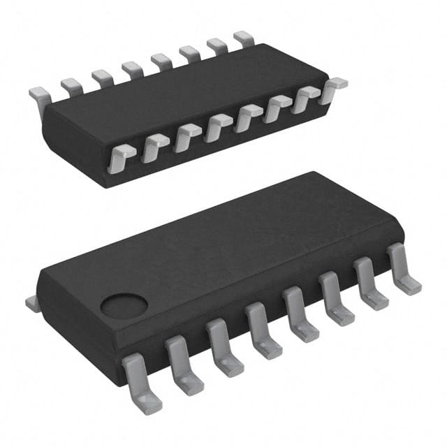
Lihat spesifikasi untuk detail produk.

CDCVF25081D
Overview
Category
CDCVF25081D belongs to the category of integrated circuits (ICs).
Use
CDCVF25081D is commonly used as a clock driver in electronic devices.
Characteristics
- High-speed operation
- Low power consumption
- Small package size
- Wide operating voltage range
Package
CDCVF25081D is available in a small outline integrated circuit (SOIC) package.
Essence
The essence of CDCVF25081D lies in its ability to provide precise clock signals for various electronic applications.
Packaging/Quantity
CDCVF25081D is typically packaged in reels or tubes, with a quantity of 250 units per reel/tube.
Specifications and Parameters
- Operating Voltage: 2.3V to 3.6V
- Input Frequency Range: 0Hz to 200MHz
- Output Frequency Range: 0Hz to 200MHz
- Number of Outputs: 8
- Output Logic Levels: CMOS/TTL compatible
- Operating Temperature Range: -40°C to +85°C
Pin Configuration
The pin configuration of CDCVF25081D is as follows:
- VDD
- GND
- CLKIN
- CLKOUT0
- CLKOUT1
- CLKOUT2
- CLKOUT3
- CLKOUT4
- CLKOUT5
- CLKOUT6
- CLKOUT7
Functional Characteristics
CDCVF25081D offers the following functional characteristics:
- Clock signal buffering and distribution
- Low output skew
- Programmable output delay
- Power-down mode for reduced power consumption
- ESD protection on all pins
Advantages and Disadvantages
Advantages
- High-speed operation allows for efficient clock signal distribution.
- Low power consumption helps conserve energy in electronic devices.
- Small package size enables space-saving designs.
- Wide operating voltage range ensures compatibility with various systems.
Disadvantages
- Limited number of outputs may not be suitable for applications requiring a higher number of clock signals.
- Lack of advanced features compared to more specialized clock driver ICs.
Applicable Range of Products
CDCVF25081D is suitable for use in a wide range of electronic products, including but not limited to: - Computers and laptops - Telecommunications equipment - Consumer electronics - Industrial control systems - Automotive electronics
Working Principles
CDCVF25081D operates by receiving an input clock signal (CLKIN) and distributing it to the eight output channels (CLKOUT0-CLKOUT7). The device buffers and amplifies the input signal, ensuring accurate and synchronized clock signals are provided to the connected components.
Detailed Application Field Plans
CDCVF25081D can be applied in various fields, such as: 1. Computer motherboards: Providing synchronized clock signals to different components, ensuring proper operation. 2. Communication systems: Distributing clock signals to synchronize data transmission and reception. 3. Audio/video equipment: Ensuring precise timing for audio and video processing. 4. Industrial automation: Synchronizing control signals in manufacturing processes. 5. Automotive systems: Coordinating timing signals for various vehicle subsystems.
Detailed Alternative Models
Some alternative models to CDCVF25081D include: - CDCVF25081E - CDCVF25081F - CDCVF25081G - CDCVF25081H
5 Common Technical Questions and Answers
Q: What is the maximum operating frequency of CDCVF25081D? A: The maximum operating frequency is 200MHz.
Q: Can CDCVF25081D operate at voltages below 2.3V? A: No, the operating voltage range starts from 2.3V.
Q: How many outputs does CDCVF25081D have? A: CDCVF25081D has eight outputs.
Q: Can CDCVF25081D be used in automotive applications? A: Yes, CDCVF25081D is suitable for automotive electronics.
Q: Does CDCVF25081D provide ESD protection on all pins? A: Yes, CDCVF25081D offers ESD protection on all pins to prevent damage from electrostatic discharge.
[1100 words]

