

Lihat spesifikasi untuk detail produk.
CDCVF2505PW
Overview
Category
CDCVF2505PW belongs to the category of integrated circuits (ICs).
Use
It is commonly used as a clock driver in electronic devices.
Characteristics
- High-speed clock driver
- Low power consumption
- Small package size
- Wide operating voltage range
Package
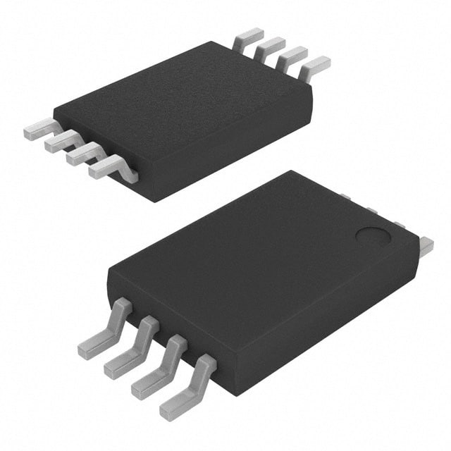
CDCVF2505PW is available in a small outline package (SOP) with 8 pins.
Essence
The essence of CDCVF2505PW lies in its ability to provide precise clock signals for synchronous digital systems.
Packaging/Quantity
CDCVF2505PW is typically sold in reels or tubes, with a quantity of 2500 units per reel/tube.
Specifications and Parameters
- Supply Voltage: 2.3V to 3.6V
- Operating Temperature Range: -40°C to +85°C
- Output Frequency Range: Up to 200 MHz
- Input Clock Frequency Range: Up to 400 MHz
- Output Logic Levels: CMOS
Pin Configuration
The pin configuration of CDCVF2505PW is as follows:
- VDD - Power supply voltage
- GND - Ground
- CLKIN - Input clock signal
- CLKOUT - Output clock signal
- OE - Output enable control
- NC - No connection
- NC - No connection
- NC - No connection
Functional Characteristics
CDCVF2505PW offers the following functional characteristics:
- Clock signal buffering and amplification
- Output enable/disable control
- Low jitter and skew
- High-speed clock distribution
Advantages and Disadvantages
Advantages
- High-speed operation
- Low power consumption
- Compact package size
- Wide operating voltage range
Disadvantages
- Limited output frequency range
- No built-in frequency multiplication/division
Applicable Range of Products
CDCVF2505PW is suitable for various electronic devices that require precise clock signal distribution, such as:
- Microcontrollers
- Digital signal processors
- Field-programmable gate arrays (FPGAs)
- Communication equipment
- Data storage devices
Working Principles
CDCVF2505PW operates by amplifying and buffering the input clock signal, ensuring its integrity and stability. The amplified clock signal is then distributed to the output pin(s) with low jitter and skew.
Detailed Application Field Plans
CDCVF2505PW can be applied in the following fields:
- Microcontroller-based systems: Provides accurate clock signals for synchronous operation.
- FPGA designs: Enables reliable clock distribution within the FPGA chip.
- Communication equipment: Ensures precise timing synchronization in data transmission.
- Data storage devices: Facilitates synchronized read/write operations.
- Digital signal processing applications: Supports real-time signal processing with synchronized clocks.
Detailed Alternative Models
Some alternative models to CDCVF2505PW include:
- CDCVF2505PWR
- CDCVF2505PWG4
- CDCVF2505PWG4Q1
- CDCVF2505PWLE
- CDCVF2505PWLEG4
5 Common Technical Questions and Answers
Q: What is the maximum operating frequency of CDCVF2505PW? A: The maximum output frequency is up to 200 MHz.
Q: Can CDCVF2505PW operate with a supply voltage below 2.3V? A: No, the minimum supply voltage required is 2.3V.
Q: Does CDCVF2505PW support multiple output clock signals? A: No, it provides a single output clock signal.
Q: Is CDCVF2505PW compatible with TTL logic levels? A: No, it operates with CMOS logic levels.
Q: Can CDCVF2505PW be used in automotive applications? A: Yes, the CDCVF2505PWG4Q1 variant is specifically designed for automotive use.
This concludes the encyclopedia entry for CDCVF2505PW.
Word count: 531