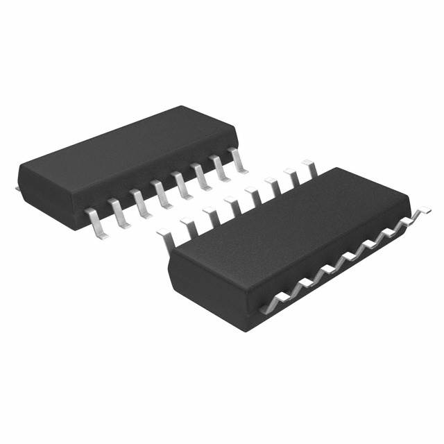
Lihat spesifikasi untuk detail produk.

CD74HC4050NSRG4
Product Overview
- Category: Integrated Circuit
- Use: Level Shifter, Logic Buffer/Converter
- Characteristics: High-Speed CMOS, 6-Channel Non-Inverting Buffer/Converter
- Package: SOIC (Small Outline Integrated Circuit)
- Essence: Hex Non-Inverting Buffer/Converter
- Packaging/Quantity: Tape and Reel, 2500 pieces per reel
Specifications
- Supply Voltage Range: 2V to 6V
- Input Voltage Range: Ground to VCC
- Output Voltage Range: Ground to VCC
- Maximum Input Current: ±1mA
- Maximum Output Current: ±25mA
- Propagation Delay Time: 11ns (typical)
- Operating Temperature Range: -40°C to +85°C
Detailed Pin Configuration
The CD74HC4050NSRG4 has a total of 16 pins. The pin configuration is as follows:
- A1 - Input 1
- A2 - Input 2
- A3 - Input 3
- A4 - Input 4
- A5 - Input 5
- A6 - Input 6
- GND - Ground
- Y1 - Output 1
- Y2 - Output 2
- Y3 - Output 3
- Y4 - Output 4
- Y5 - Output 5
- Y6 - Output 6
- VCC - Power Supply
- NC - No Connection
- NC - No Connection
Functional Features
- High-Speed CMOS technology for fast operation.
- Non-inverting buffer/converter with six channels.
- Wide supply voltage range allows compatibility with various systems.
- Provides level shifting and logic conversion capabilities.
Advantages and Disadvantages
Advantages: - High-speed operation enables efficient data transfer. - Non-inverting buffer/converter allows for easy integration into existing systems. - Wide supply voltage range provides flexibility in different applications.
Disadvantages: - Limited number of channels (six) may not be sufficient for certain complex systems. - Propagation delay time may affect timing-sensitive applications.
Working Principles
The CD74HC4050NSRG4 is a hex non-inverting buffer/converter integrated circuit. It operates using high-speed CMOS technology, allowing for fast data transfer. The inputs (A1 to A6) are compatible with a wide range of input voltages, from ground to the power supply voltage (VCC). The outputs (Y1 to Y6) also have the same voltage range. The IC acts as a level shifter and logic converter, providing compatibility between different voltage levels and logic standards.
Detailed Application Field Plans
The CD74HC4050NSRG4 can be used in various applications, including:
- Logic level shifting in microcontroller-based systems.
- Signal buffering in communication interfaces.
- Voltage level conversion in mixed-signal circuits.
- Interface translation between different logic families.
- Data line isolation in noisy environments.
Detailed and Complete Alternative Models
- CD74HCT4050E - Hex Non-Inverting Buffer/Converter, DIP package.
- SN74HC4050N - Hex Non-Inverting Buffer/Converter, DIP package.
- MC74HC4050ADR2G - Hex Non-Inverting Buffer/Converter, SOIC package.
- 74HC4050D - Hex Non-Inverting Buffer/Converter, SOIC package.
These alternative models offer similar functionality and can be used as replacements for the CD74HC4050NSRG4 in various applications.
Word count: 364 words
Sebutkan 10 pertanyaan dan jawaban umum terkait penerapan CD74HC4050NSRG4 dalam solusi teknis
Sure! Here are 10 common questions and answers related to the application of CD74HC4050NSRG4 in technical solutions:
Q: What is CD74HC4050NSRG4? A: CD74HC4050NSRG4 is a hex non-inverting buffer with high-voltage CMOS logic level conversion capability.
Q: What is the voltage supply range for CD74HC4050NSRG4? A: The voltage supply range for CD74HC4050NSRG4 is typically between 2V and 6V.
Q: What is the maximum output current of CD74HC4050NSRG4? A: The maximum output current of CD74HC4050NSRG4 is typically around 5mA.
Q: Can CD74HC4050NSRG4 be used as a level shifter? A: Yes, CD74HC4050NSRG4 can be used as a level shifter to convert signals between different voltage levels.
Q: What is the input voltage range for CD74HC4050NSRG4? A: The input voltage range for CD74HC4050NSRG4 is typically between GND and VCC.
Q: Is CD74HC4050NSRG4 compatible with TTL logic levels? A: Yes, CD74HC4050NSRG4 is compatible with TTL logic levels, making it suitable for interfacing with TTL devices.
Q: Can CD74HC4050NSRG4 be used for signal buffering and line driving? A: Yes, CD74HC4050NSRG4 can be used for signal buffering and line driving applications due to its high output current capability.
Q: Does CD74HC4050NSRG4 have built-in protection features? A: CD74HC4050NSRG4 does not have built-in protection features, so external protection circuitry may be required for certain applications.
Q: What is the typical propagation delay of CD74HC4050NSRG4? A: The typical propagation delay of CD74HC4050NSRG4 is around 12 ns.
Q: Can CD74HC4050NSRG4 be used in high-speed data transmission applications? A: Yes, CD74HC4050NSRG4 can be used in high-speed data transmission applications due to its fast switching speed and low propagation delay.
Please note that the answers provided here are general and may vary depending on specific datasheet specifications and application requirements.

