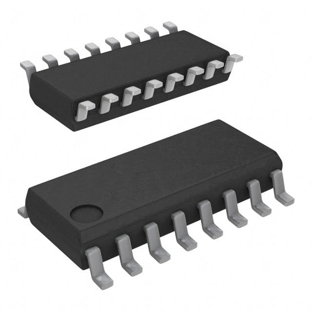
Lihat spesifikasi untuk detail produk.

CD74HC109ME4
Product Overview
- Category: Integrated Circuit (IC)
- Use: Digital Logic
- Characteristics: Dual J-K Flip-Flop with Clear and Preset, High-Speed CMOS Logic
- Package: SOIC-16
- Essence: Flip-flop circuitry for storing and manipulating digital data
- Packaging/Quantity: Tape and Reel, 2500 units per reel
Specifications
- Supply Voltage Range: 2V to 6V
- High-Level Input Voltage: 2V
- Low-Level Input Voltage: 0.8V
- High-Level Output Current: -5.2mA
- Low-Level Output Current: 5.2mA
- Maximum Operating Frequency: 74MHz
- Propagation Delay Time: 9ns
- Operating Temperature Range: -40°C to +85°C
Detailed Pin Configuration
- CLR (Clear) - Active LOW input for clearing the flip-flop
- PR (Preset) - Active LOW input for presetting the flip-flop
- CP (Clock Pulse) - Clock input for synchronizing the flip-flop
- D (Data) - Data input for setting the flip-flop state
- Q1 (Output 1) - Output of the first flip-flop
- Q1̅ (Complementary Output 1) - Complementary output of the first flip-flop
- GND (Ground) - Ground reference for the IC
- Q2 (Output 2) - Output of the second flip-flop
- Q2̅ (Complementary Output 2) - Complementary output of the second flip-flop
- VCC (Supply Voltage) - Positive supply voltage for the IC
- NC (No Connection) - No internal connection, can be left unconnected
- NC (No Connection) - No internal connection, can be left unconnected
- J1 (J-K Input 1) - J-K input for the first flip-flop
- K1 (J-K Input 1) - J-K input for the first flip-flop
- J2 (J-K Input 2) - J-K input for the second flip-flop
- K2 (J-K Input 2) - J-K input for the second flip-flop
Functional Features
- Dual J-K Flip-Flop: Contains two independent J-K flip-flops in a single IC package.
- Clear and Preset Inputs: Allows for clearing or presetting the flip-flop to a specific state.
- High-Speed CMOS Logic: Operates at high frequencies with low power consumption.
- Wide Supply Voltage Range: Can be powered by a range of 2V to 6V, providing flexibility in different applications.
Advantages and Disadvantages
Advantages: - Compact Design: Integration of two flip-flops in a single package saves board space. - Versatile Functionality: Clear and preset inputs enhance the flexibility of the flip-flop. - High-Speed Operation: Suitable for applications requiring fast data storage and manipulation.
Disadvantages: - Limited Output Current: The maximum output current is relatively low, which may restrict certain applications. - Temperature Sensitivity: Performance may vary under extreme temperature conditions.
Working Principles
The CD74HC109ME4 is based on J-K flip-flop circuitry. It stores and manipulates digital data using clocked inputs and outputs. The flip-flop can be cleared or preset to a specific state using the clear and preset inputs. The clock pulse synchronizes the flip-flop, allowing data to be stored or transferred based on the input signals. The complementary outputs provide inverted versions of the main outputs, enhancing flexibility in circuit design.
Detailed Application Field Plans
The CD74HC109ME4 is widely used in various digital logic applications, including but not limited to: - Counters and Registers: Used for storing and manipulating binary data in sequential circuits. - Data Storage Systems: Enables efficient data storage and retrieval in memory systems. - Control Systems: Provides flip-flop functionality for controlling and sequencing operations. - Communication Systems: Facilitates data transmission and reception in digital communication protocols.
Detailed and Complete Alternative Models
- SN74HC109N: Similar dual J-K flip-flop IC with clear and preset inputs, available in DIP-16 package.
- MC74HC109: Dual J-K flip-flop IC with clear and preset inputs, available in SOIC-16 package.
- CD4013BE: Dual D-type flip-flop IC with clear input, available in DIP-14 package.
- 74LS73: Dual negative-edge-triggered J-K flip-flop IC, available in DIP-14 package.
These alternative models offer similar functionality and can be
Sebutkan 10 pertanyaan dan jawaban umum terkait penerapan CD74HC109ME4 dalam solusi teknis
Sure! Here are 10 common questions and answers related to the application of CD74HC109ME4 in technical solutions:
Q: What is CD74HC109ME4? A: CD74HC109ME4 is a dual J-K flip-flop integrated circuit (IC) that can be used in various digital applications.
Q: What is the operating voltage range for CD74HC109ME4? A: The operating voltage range for CD74HC109ME4 is typically between 2V and 6V.
Q: What is the maximum clock frequency supported by CD74HC109ME4? A: CD74HC109ME4 can support clock frequencies up to 50 MHz.
Q: How many flip-flops are there in CD74HC109ME4? A: CD74HC109ME4 contains two independent J-K flip-flops.
Q: What is the purpose of the J and K inputs in CD74HC109ME4? A: The J and K inputs are used to control the state of the flip-flops. They determine whether the output will toggle, hold, or reset based on the clock input.
Q: Can CD74HC109ME4 be used in synchronous or asynchronous mode? A: CD74HC109ME4 can be used in both synchronous and asynchronous modes, depending on the application requirements.
Q: What is the typical propagation delay of CD74HC109ME4? A: The typical propagation delay of CD74HC109ME4 is around 9 ns.
Q: Is CD74HC109ME4 compatible with TTL logic levels? A: Yes, CD74HC109ME4 is compatible with TTL logic levels, making it suitable for interfacing with other TTL devices.
Q: Can CD74HC109ME4 be used in high-speed applications? A: Yes, CD74HC109ME4 is designed for high-speed operation and can be used in various high-frequency applications.
Q: What are some common applications of CD74HC109ME4? A: CD74HC109ME4 can be used in counters, frequency dividers, shift registers, data storage, and other digital logic circuits.
Please note that the answers provided here are general and may vary depending on specific datasheet specifications and application requirements.

