Lihat spesifikasi untuk detail produk.

CD4009UBNSRE4
Product Overview
Category
CD4009UBNSRE4 belongs to the category of integrated circuits (ICs).
Use
It is commonly used in electronic circuits for signal processing and amplification.
Characteristics
- CD4009UBNSRE4 is a hex inverter/buffer IC.
- It operates at a wide voltage range, typically from 3V to 18V.
- The IC has high noise immunity and low power consumption.
- It is designed to be compatible with both TTL and CMOS logic levels.
Package
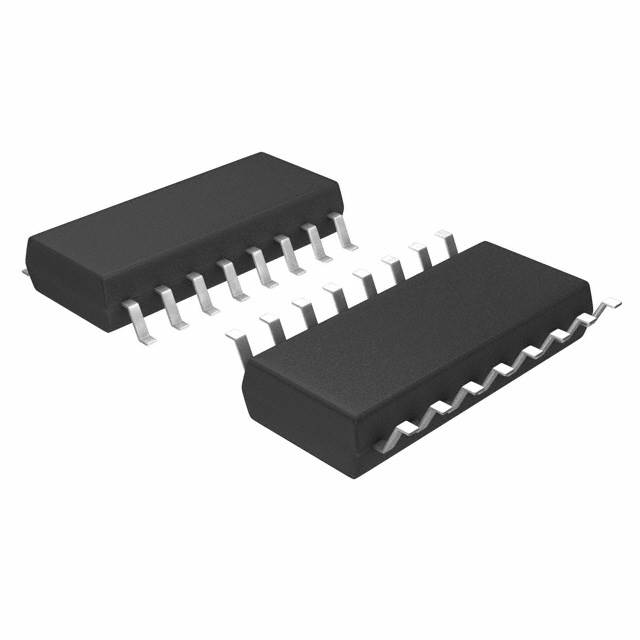
CD4009UBNSRE4 is available in a standard SOIC (Small Outline Integrated Circuit) package.
Essence
The essence of CD4009UBNSRE4 lies in its ability to invert or buffer input signals, making it an essential component in digital electronics.
Packaging/Quantity
The IC is typically sold in reels containing a quantity of 2500 units.
Specifications
- Supply Voltage Range: 3V to 18V
- Input Voltage Range: 0V to VDD
- Output Voltage Range: 0V to VDD
- Maximum Operating Frequency: 5 MHz
- Propagation Delay Time: 60 ns (max)
- Operating Temperature Range: -55°C to +125°C
Detailed Pin Configuration
CD4009UBNSRE4 consists of 14 pins arranged as follows:
__    __
   1 | 1  \/  14 | VDD
   2 | 2      13 | Output 6
   3 | 3      12 | Input 6
   4 | 4      11 | Output 5
   5 | 5      10 | Input 5
   6 | 6       9 | Output 4
   7 | 7       8 | Input 4
       ----------
Functional Features
- CD4009UBNSRE4 provides six independent inverters/buffers.
- Each inverter/buffer has a separate input and output pin.
- The IC can be used to invert or buffer digital signals.
- It has high noise immunity, making it suitable for noisy environments.
- CD4009UBNSRE4 is compatible with both TTL and CMOS logic levels.
Advantages and Disadvantages
Advantages
- Wide voltage range allows for versatile applications.
- High noise immunity ensures reliable signal processing.
- Low power consumption makes it energy-efficient.
- Compatibility with TTL and CMOS logic levels enhances flexibility.
Disadvantages
- Limited maximum operating frequency of 5 MHz.
- Propagation delay time may affect real-time applications.
Working Principles
CD4009UBNSRE4 operates based on the principles of digital logic. When an input signal is applied to one of the inverters/buffers, it either inverts the signal or buffers it without inversion, depending on the desired configuration. The output signal is then obtained from the corresponding output pin.
Detailed Application Field Plans
CD4009UBNSRE4 finds applications in various fields, including:
- Digital electronics: Used in logic circuits, microcontrollers, and digital signal processing systems.
- Communication systems: Employed in data transmission and reception circuits.
- Industrial automation: Integrated into control systems and sensor interfaces.
- Automotive electronics: Utilized in vehicle control units and electronic subsystems.
- Consumer electronics: Incorporated in audio/video equipment and home automation systems.
Detailed and Complete Alternative Models
Some alternative models that can be considered as replacements for CD4009UBNSRE4 are:
- CD4049UB: Hex inverter/buffer IC with similar characteristics and pin configuration.
- SN74LS04: Hex inverter IC with TTL logic levels.
- MC14069UB: Hex inverter/buffer IC with CMOS logic levels.
These alternative models offer similar functionality and can be used as substitutes depending on specific requirements.
Word count: 529 words
Sebutkan 10 pertanyaan dan jawaban umum terkait penerapan CD4009UBNSRE4 dalam solusi teknis
Sure! Here are 10 common questions and answers related to the application of CD4009UBNSRE4 in technical solutions:
Q: What is CD4009UBNSRE4? A: CD4009UBNSRE4 is a hex inverter/buffer IC (integrated circuit) that can be used in various digital logic applications.
Q: What is the voltage supply range for CD4009UBNSRE4? A: The voltage supply range for CD4009UBNSRE4 is typically between 3V and 18V.
Q: Can CD4009UBNSRE4 be used as a level shifter? A: Yes, CD4009UBNSRE4 can be used as a level shifter to convert signals between different voltage levels.
Q: How many inverters are there in CD4009UBNSRE4? A: CD4009UBNSRE4 contains six independent inverters.
Q: What is the maximum output current of CD4009UBNSRE4? A: The maximum output current of CD4009UBNSRE4 is typically around 6mA.
Q: Can CD4009UBNSRE4 be used in high-speed applications? A: CD4009UBNSRE4 is not specifically designed for high-speed applications, but it can be used in moderate-speed digital circuits.
Q: Is CD4009UBNSRE4 compatible with TTL (Transistor-Transistor Logic) inputs? A: Yes, CD4009UBNSRE4 is compatible with TTL inputs and can be used in TTL-compatible circuits.
Q: What is the operating temperature range for CD4009UBNSRE4? A: The operating temperature range for CD4009UBNSRE4 is typically between -55°C and 125°C.
Q: Can CD4009UBNSRE4 be used in battery-powered applications? A: Yes, CD4009UBNSRE4 can be used in battery-powered applications as it operates within a wide voltage supply range.
Q: Are there any recommended application circuits available for CD4009UBNSRE4? A: Yes, the datasheet of CD4009UBNSRE4 provides several recommended application circuits that can help in designing with this IC.
Please note that these answers are general and may vary depending on specific design requirements and conditions. It is always recommended to refer to the datasheet and consult with technical experts for accurate information and guidance.

