

Lihat spesifikasi untuk detail produk.
ADS5433IPJYG3
Product Overview
Category
The ADS5433IPJYG3 belongs to the category of analog-to-digital converters (ADCs).
Use
This product is primarily used for converting analog signals into digital format, enabling accurate and precise measurements in various applications.
Characteristics
- High-speed conversion: The ADS5433IPJYG3 offers fast conversion rates, allowing for real-time data acquisition.
- High resolution: It provides high-resolution digitization, ensuring accurate representation of analog signals.
- Low power consumption: The device is designed to operate efficiently with minimal power consumption.
- Wide input voltage range: The ADC can handle a wide range of input voltages, making it suitable for diverse signal sources.
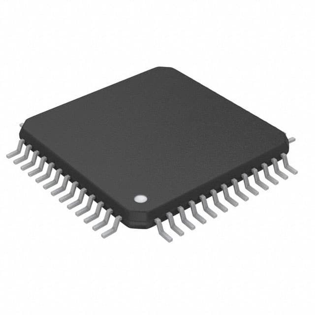
Package
The ADS5433IPJYG3 comes in a compact package, which ensures easy integration into electronic systems. The package type is PJY, and it is lead-free.
Essence
The essence of the ADS5433IPJYG3 lies in its ability to convert analog signals into digital form accurately and rapidly, facilitating precise measurements and analysis.
Packaging/Quantity
The product is typically packaged in reels or tubes, containing a specific quantity of ADCs per package. The exact packaging and quantity may vary depending on the supplier.
Specifications
- Resolution: 12 bits
- Sampling Rate: Up to 100 MSPS (Mega Samples Per Second)
- Input Voltage Range: ±5V
- Power Supply: +5V
- Operating Temperature Range: -40°C to +85°C
- Interface: Parallel
Detailed Pin Configuration
The ADS5433IPJYG3 has the following pin configuration:
- VREFP: Positive reference voltage input
- VREFN: Negative reference voltage input
- VIN: Analog input
- CLK: Clock input
- CS: Chip select input
- D[11:0]: Digital output
- GND: Ground
- VDD: Power supply
Functional Features
- High-speed conversion: The ADC offers fast and accurate conversion of analog signals into digital form.
- Low power consumption: It operates efficiently with minimal power requirements.
- Wide input voltage range: The device can handle a wide range of input voltages, making it versatile for various applications.
- Parallel interface: The ADC utilizes a parallel interface for easy integration with microcontrollers or other digital systems.
Advantages and Disadvantages
Advantages
- Fast conversion rate enables real-time data acquisition.
- High resolution ensures accurate representation of analog signals.
- Low power consumption results in energy-efficient operation.
- Wide input voltage range allows for compatibility with diverse signal sources.
Disadvantages
- Limited to parallel interface, which may not be suitable for all applications.
- Higher cost compared to lower-end ADCs with similar specifications.
Working Principles
The ADS5433IPJYG3 operates based on the principle of successive approximation. It samples the analog input signal at a high rate and converts it into a digital representation using a 12-bit resolution. The conversion process involves comparing the input voltage against a reference voltage and iteratively adjusting the digital output until an accurate representation is achieved.
Detailed Application Field Plans
The ADS5433IPJYG3 finds applications in various fields, including:
- Communications: Used in wireless communication systems for signal processing and modulation/demodulation.
- Test and Measurement: Enables precise measurements in scientific instruments, oscilloscopes, and data acquisition systems.
- Industrial Automation: Utilized for monitoring and control purposes in industrial processes.
- Medical Equipment: Enables accurate measurement and analysis in medical devices such as ultrasound machines and patient monitors.
- Audio Processing: Used in professional audio equipment for high-fidelity signal conversion.
Detailed and Complete Alternative Models
- ADS5433IPJYR: Similar to ADS5433IPJYG3, but with a different package type (PJYR).
- ADS5433IPJYG4: Upgraded version with improved specifications and features.
- ADS5433IPJYF3: Lower-cost alternative with slightly reduced performance.
These alternative models offer similar functionality and can be considered based on specific requirements and budget constraints.
Word count: 570 words
Sebutkan 10 pertanyaan dan jawaban umum terkait penerapan ADS5433IPJYG3 dalam solusi teknis
Sure! Here are 10 common questions and answers related to the application of ADS5433IPJYG3 in technical solutions:
Q: What is the ADS5433IPJYG3? A: The ADS5433IPJYG3 is a high-speed, low-power, 12-bit analog-to-digital converter (ADC) designed for use in various technical applications.
Q: What is the maximum sampling rate of the ADS5433IPJYG3? A: The ADS5433IPJYG3 has a maximum sampling rate of 210 MSPS (Mega Samples Per Second).
Q: What is the power supply voltage range for the ADS5433IPJYG3? A: The ADS5433IPJYG3 operates with a power supply voltage range of 1.8V to 3.6V.
Q: Can the ADS5433IPJYG3 be used in battery-powered devices? A: Yes, the low-power design of the ADS5433IPJYG3 makes it suitable for battery-powered devices.
Q: What is the input voltage range of the ADS5433IPJYG3? A: The ADS5433IPJYG3 has a differential input voltage range of -0.5V to +2.0V.
Q: Does the ADS5433IPJYG3 have built-in digital signal processing features? A: No, the ADS5433IPJYG3 is a standalone ADC and does not have built-in digital signal processing features.
Q: What is the output interface of the ADS5433IPJYG3? A: The ADS5433IPJYG3 provides a parallel CMOS output interface.
Q: Can the ADS5433IPJYG3 be used in high-frequency applications? A: Yes, the ADS5433IPJYG3 is designed for high-speed applications and can be used in high-frequency systems.
Q: What is the typical power consumption of the ADS5433IPJYG3? A: The typical power consumption of the ADS5433IPJYG3 is around 300 mW (milliwatts).
Q: Are evaluation boards or reference designs available for the ADS5433IPJYG3? A: Yes, Texas Instruments provides evaluation boards and reference designs to help users get started with the ADS5433IPJYG3 in their technical solutions.
Please note that these answers are general and may vary depending on specific application requirements. It is always recommended to refer to the datasheet and consult with the manufacturer for accurate information.