

Lihat spesifikasi untuk detail produk.
ADC102S021CIMM
Product Overview
- Category: Analog-to-Digital Converter (ADC)
- Use: Converts analog signals into digital data for processing and analysis
- Characteristics: High resolution, low power consumption, small package size
- Package: Integrated Circuit (IC)
- Essence: Converts continuous analog signals into discrete digital values
- Packaging/Quantity: Available in tape and reel packaging, quantity varies based on supplier
Specifications
- Resolution: 10 bits
- Sampling Rate: Up to 200 kilosamples per second (ksps)
- Input Voltage Range: 0V to VREF
- Power Supply: 2.7V to 5.5V
- Operating Temperature Range: -40°C to +125°C
- Interface: Serial Peripheral Interface (SPI)
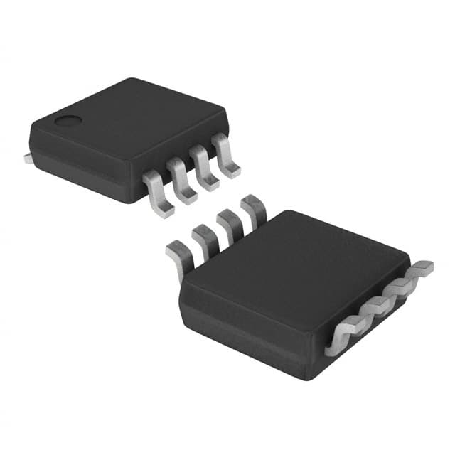
Detailed Pin Configuration
The ADC102S021CIMM has a total of 16 pins:
- VDD: Power supply voltage
- GND: Ground reference
- REF: Reference voltage input
- AGND: Analog ground reference
- VIN+: Positive analog input voltage
- VIN-: Negative analog input voltage
- CLK: Clock input for SPI communication
- CS: Chip select input for SPI communication
- DOUT: Digital output data
- DIN: Digital input data
- SCLK: Serial clock input for SPI communication
- SDI: Serial data input for SPI communication
- SDO: Serial data output for SPI communication
- EOC: End of conversion output
- NC: No connection
- VREF: Reference voltage output
Functional Features
- High-resolution conversion with 10-bit accuracy
- Low power consumption for energy-efficient operation
- Small package size allows for space-saving integration
- Serial Peripheral Interface (SPI) enables easy communication with microcontrollers
- End of conversion output signal for synchronization
Advantages and Disadvantages
Advantages
- High resolution provides accurate digital representation of analog signals
- Low power consumption extends battery life in portable applications
- Small package size allows for integration in space-constrained designs
- SPI interface simplifies communication with microcontrollers
Disadvantages
- Limited input voltage range may not be suitable for high-voltage applications
- Lower sampling rate compared to some other ADC models
- Requires external reference voltage for accurate conversion
Working Principles
The ADC102S021CIMM operates on the principle of successive approximation. It samples the analog input voltage and compares it to a reference voltage. By iteratively adjusting the digital code, it converges towards the closest digital representation of the analog signal. The conversion process is controlled by an internal clock and can be triggered by an external signal.
Detailed Application Field Plans
The ADC102S021CIMM finds applications in various fields, including:
- Industrial automation: Monitoring and control systems that require precise analog-to-digital conversion.
- Medical devices: Accurate measurement of physiological signals for diagnostics and treatment.
- Communication systems: Signal processing and modulation/demodulation applications.
- Automotive electronics: Sensor data acquisition and control systems.
- Consumer electronics: Audio and video signal processing, touch screen interfaces.
Detailed and Complete Alternative Models
- ADC101S021CIMM: Similar specifications but with 10-bit resolution.
- ADC103S021CIMM: Higher resolution with 12-bit accuracy.
- ADC102S051CIMM: Same resolution but higher sampling rate of 500 ksps.
- ADC102S071CIMM: Extended temperature range (-40°C to +150°C) for harsh environments.
These alternative models offer different trade-offs in terms of resolution, sampling rate, and temperature range, allowing designers to choose the most suitable option for their specific application requirements.
Word count: 496 words
Sebutkan 10 pertanyaan dan jawaban umum terkait penerapan ADC102S021CIMM dalam solusi teknis
Sure! Here are 10 common questions and answers related to the application of ADC102S021CIMM in technical solutions:
Q: What is ADC102S021CIMM? A: ADC102S021CIMM is a dual-channel, 10-bit analog-to-digital converter (ADC) integrated circuit.
Q: What is the operating voltage range of ADC102S021CIMM? A: The operating voltage range of ADC102S021CIMM is typically between 2.7V and 5.5V.
Q: What is the maximum sampling rate of ADC102S021CIMM? A: The maximum sampling rate of ADC102S021CIMM is 200 kilosamples per second (ksps).
Q: What is the resolution of ADC102S021CIMM? A: ADC102S021CIMM has a resolution of 10 bits, which means it can represent analog signals with 2^10 (1024) discrete levels.
Q: What is the input voltage range of ADC102S021CIMM? A: The input voltage range of ADC102S021CIMM is typically between 0V and VREF, where VREF is the reference voltage.
Q: Does ADC102S021CIMM support differential inputs? A: Yes, ADC102S021CIMM supports differential inputs, allowing for better noise rejection and increased dynamic range.
Q: What is the power consumption of ADC102S021CIMM? A: The power consumption of ADC102S021CIMM depends on the operating conditions but is typically around 1 milliwatt (mW).
Q: Can ADC102S021CIMM operate in a low-power mode? A: Yes, ADC102S021CIMM has a low-power mode that reduces the power consumption when not actively sampling.
Q: What is the interface used to communicate with ADC102S021CIMM? A: ADC102S021CIMM uses a serial interface called Serial Peripheral Interface (SPI) for communication with a microcontroller or other devices.
Q: Can ADC102S021CIMM be used in battery-powered applications? A: Yes, ADC102S021CIMM's low power consumption and wide operating voltage range make it suitable for battery-powered applications.
Please note that the answers provided here are general and may vary depending on specific datasheet specifications and application requirements.