

Lihat spesifikasi untuk detail produk.
HCF40107M013TR
Product Overview
Category
HCF40107M013TR belongs to the category of integrated circuits (ICs).
Use
This product is commonly used in electronic devices for various applications, including signal processing and control systems.
Characteristics
- Integrated circuit
- High reliability
- Low power consumption
- Wide operating voltage range
- Compact package size
Package
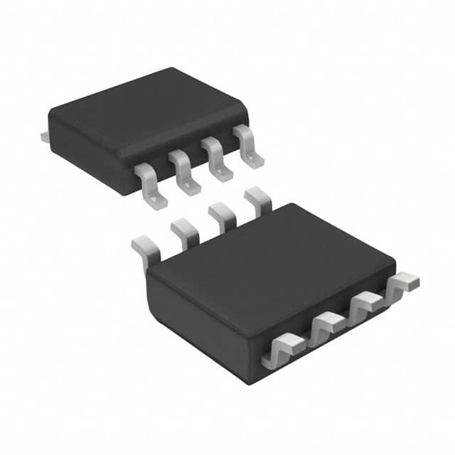
HCF40107M013TR is available in a small outline package (SOP) with a specific pin configuration.
Essence
The essence of HCF40107M013TR lies in its ability to perform multiple functions within a single integrated circuit, simplifying circuit design and reducing component count.
Packaging/Quantity
This product is typically packaged in reels or tubes, with a quantity of 2500 units per reel/tube.
Specifications
- Supply Voltage: 3V - 18V
- Operating Temperature Range: -40°C to +85°C
- Logic Family: CMOS
- Number of Pins: 16
- Input/Output Type: Single-ended
Detailed Pin Configuration
- VDD - Positive power supply
- GND - Ground reference
- A - Input A
- B - Input B
- C - Input C
- D - Input D
- CLR - Clear input
- CLK - Clock input
- QD - Output QD
- QC - Output QC
- QB - Output QB
- QA - Output QA
- QD' - Complementary output QD
- QC' - Complementary output QC
- QB' - Complementary output QB
- QA' - Complementary output QA
Functional Features
- Quad 2-input NAND gates with Schmitt-trigger inputs
- Buffered outputs for improved noise immunity
- Schmitt-trigger inputs provide hysteresis for increased noise immunity and signal shaping capabilities
Advantages and Disadvantages
Advantages
- High reliability due to integrated design
- Low power consumption, making it suitable for battery-powered devices
- Wide operating voltage range allows compatibility with various systems
- Compact package size saves board space and facilitates miniaturization
Disadvantages
- Limited number of input/output pins may restrict complex circuit designs
- CMOS logic family may have lower speed compared to other families like TTL
Working Principles
HCF40107M013TR operates based on the principles of digital logic. The quad 2-input NAND gates receive input signals and perform logical operations, producing corresponding output signals. The Schmitt-trigger inputs ensure reliable switching behavior by providing hysteresis and noise immunity.
Detailed Application Field Plans
HCF40107M013TR finds applications in a wide range of electronic systems, including: 1. Signal processing circuits 2. Control systems 3. Data communication devices 4. Industrial automation equipment 5. Consumer electronics
Detailed and Complete Alternative Models
- HCF40106M013TR - Hex Schmitt-trigger inverters
- HCF4011M013TR - Quad 2-input NAND gates
- HCF4013M013TR - Dual D-type flip-flops
These alternative models offer similar functionality and can be used as substitutes for HCF40107M013TR in various applications.
Word count: 446 words
Sebutkan 10 pertanyaan dan jawaban umum terkait penerapan HCF40107M013TR dalam solusi teknis
Sure! Here are 10 common questions and answers related to the application of HCF40107M013TR in technical solutions:
Q: What is HCF40107M013TR? A: HCF40107M013TR is a specific model of integrated circuit (IC) that belongs to the HCF series of logic gates.
Q: What is the purpose of HCF40107M013TR? A: HCF40107M013TR is primarily used as a hex buffer/driver IC, which can be employed to amplify or buffer digital signals.
Q: What voltage levels does HCF40107M013TR support? A: HCF40107M013TR operates with a supply voltage range of 3V to 18V.
Q: How many buffers/drivers are there in HCF40107M013TR? A: HCF40107M013TR consists of six independent buffers/drivers, each capable of handling one input signal.
Q: Can HCF40107M013TR handle both TTL and CMOS inputs? A: Yes, HCF40107M013TR is compatible with both TTL (Transistor-Transistor Logic) and CMOS (Complementary Metal-Oxide-Semiconductor) input levels.
Q: What is the maximum output current of HCF40107M013TR? A: The maximum output current per buffer/driver in HCF40107M013TR is typically around 25mA.
Q: Does HCF40107M013TR have any built-in protection features? A: Yes, HCF40107M013TR includes built-in protection against electrostatic discharge (ESD) and excessive power dissipation.
Q: Can HCF40107M013TR be used in high-speed applications? A: Yes, HCF40107M013TR is designed to operate at relatively high speeds, making it suitable for many digital applications.
Q: What is the operating temperature range of HCF40107M013TR? A: HCF40107M013TR can typically operate within a temperature range of -40°C to 125°C.
Q: Are there any specific precautions to consider when using HCF40107M013TR? A: It is important to follow the manufacturer's datasheet and guidelines for proper handling, storage, and circuit design to ensure optimal performance and reliability of HCF40107M013TR.
Please note that the answers provided here are general and may vary depending on the specific application or context.