

Lihat spesifikasi untuk detail produk.
BU4093BFV-E2
Product Overview
Category: Integrated Circuit (IC)
Use: The BU4093BFV-E2 is a quad 2-input NAND gate IC, commonly used in digital logic circuits. It is designed to perform logical operations on binary inputs and produce corresponding output signals.
Characteristics: - Quad 2-input NAND gate - High-speed operation - Low power consumption - Wide operating voltage range - Compact package size
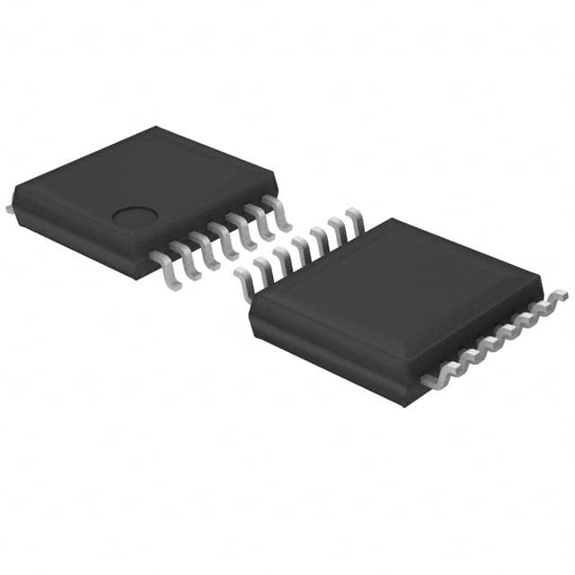
Package: The BU4093BFV-E2 is available in a small surface-mount package, making it suitable for compact electronic devices.
Essence: The essence of the BU4093BFV-E2 lies in its ability to perform logical operations using NAND gates, which are fundamental building blocks in digital circuits.
Packaging/Quantity: The BU4093BFV-E2 is typically sold in reels or tubes, with a quantity of 2500 units per reel/tube.
Specifications
- Supply Voltage Range: 3V to 18V
- Input Voltage Range: 0V to VDD
- Output Voltage Range: 0V to VDD
- Operating Temperature Range: -40°C to +85°C
- Propagation Delay Time: 10ns (max)
- Quiescent Current: 1μA (max)
Pin Configuration
The BU4093BFV-E2 has a total of 14 pins, numbered as follows:
__    __
  | 1|__|14|
  | 2|__|13|
  | 3|__|12|
  | 4|__|11|
  | 5|__|10|
  | 6|__|9 |
  | 7|__|8 |
Pin Description: 1. Input A1 2. Input B1 3. Output Y1 4. Input A2 5. Input B2 6. Output Y2 7. Ground (GND) 8. Input B3 9. Input A3 10. Output Y3 11. Input B4 12. Input A4 13. Output Y4 14. VDD (Supply Voltage)
Functional Features
- Quad 2-input NAND gate functionality: The BU4093BFV-E2 integrates four independent 2-input NAND gates in a single IC, allowing for efficient implementation of logical operations.
- High-speed operation: The IC is designed to operate at high speeds, making it suitable for applications that require quick response times.
- Low power consumption: The BU4093BFV-E2 consumes minimal power, contributing to energy-efficient designs.
- Wide operating voltage range: The IC can operate within a wide voltage range, providing flexibility in various electronic systems.
Advantages and Disadvantages
Advantages: - Compact size: The small package size of the BU4093BFV-E2 enables its use in space-constrained applications. - Versatility: The quad 2-input NAND gate configuration allows for versatile logic circuit designs. - High-speed operation: The IC's fast operation ensures efficient performance in time-critical applications.
Disadvantages: - Limited number of gates: The BU4093BFV-E2 only provides four NAND gates, which may be insufficient for complex logic circuits requiring more gates. - Lack of built-in protection features: The IC does not include built-in protection against overvoltage or electrostatic discharge, requiring additional external measures for reliable operation.
Working Principles
The BU4093BFV-E2 operates based on the principles of digital logic. Each of the four NAND gates within the IC takes two binary inputs and produces an output signal based on the logical operation performed. The NAND gate performs a logical AND operation on the inputs and then negates the result, producing a high output only when both inputs are low.
Detailed Application Field Plans
The BU4093BFV-E2 finds applications in various fields, including but not limited to: - Digital electronics - Microcontrollers - Communication systems - Consumer electronics - Industrial automation
Detailed and Complete Alternative Models
Some alternative models that can be considered as alternatives to the BU4093BFV-E2 include: - CD4011B: Quad 2-input NAND gate IC from Texas Instruments - MC14011B: Quad 2-input NAND gate IC from ON Semiconductor - HCF4093: Quad 2-input NAND gate IC from STMicroelectronics
These alternative models offer similar functionality and can be used as replacements for the BU4093BFV-E2 in various applications.
Word count: 570 words
Sebutkan 10 pertanyaan dan jawaban umum terkait penerapan BU4093BFV-E2 dalam solusi teknis
Sure! Here are 10 common questions and answers related to the application of BU4093BFV-E2 in technical solutions:
Q: What is BU4093BFV-E2? A: BU4093BFV-E2 is a quad 2-input NAND gate IC (integrated circuit) that can be used in various electronic applications.
Q: What is the operating voltage range for BU4093BFV-E2? A: The operating voltage range for BU4093BFV-E2 is typically between 3V and 18V.
Q: Can BU4093BFV-E2 be used in low-power applications? A: Yes, BU4093BFV-E2 is designed to operate at low power consumption levels, making it suitable for low-power applications.
Q: How many NAND gates are there in BU4093BFV-E2? A: BU4093BFV-E2 consists of four independent NAND gates, each with two inputs.
Q: What is the maximum output current of BU4093BFV-E2? A: The maximum output current of BU4093BFV-E2 is typically around 6mA.
Q: Can BU4093BFV-E2 be used in high-speed applications? A: While BU4093BFV-E2 is not specifically designed for high-speed applications, it can still be used in moderate-speed digital circuits.
Q: Is BU4093BFV-E2 compatible with CMOS logic levels? A: Yes, BU4093BFV-E2 operates on CMOS logic levels, making it compatible with other CMOS devices.
Q: What is the temperature range for BU4093BFV-E2? A: BU4093BFV-E2 is typically rated for operation within a temperature range of -40°C to 85°C.
Q: Can BU4093BFV-E2 be used in battery-powered devices? A: Yes, BU4093BFV-E2's low power consumption and wide operating voltage range make it suitable for battery-powered applications.
Q: What are some common applications of BU4093BFV-E2? A: BU4093BFV-E2 can be used in various digital logic circuits, such as signal conditioning, waveform generation, data processing, and more.
Please note that the answers provided here are general and may vary depending on specific datasheet specifications and application requirements.