

Lihat spesifikasi untuk detail produk.
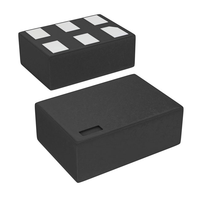
NC7SP17L6X
Product Overview
- Category: Integrated Circuit
- Use: Logic Gate
- Characteristics: Low Voltage, High-Speed, Tiny Package
- Package: SOT-23-6
- Essence: Single Schmitt-Trigger Inverter
- Packaging/Quantity: Tape and Reel, 3000 units per reel
Specifications
- Supply Voltage: 1.65V to 5.5V
- Input Voltage: 0V to VCC
- Output Voltage: 0V to VCC
- Operating Temperature: -40°C to +85°C
- Propagation Delay: 3.5ns (typical)
- Quiescent Current: 2μA (maximum)
Detailed Pin Configuration
The NC7SP17L6X is a 6-pin integrated circuit with the following pin configuration:
- Pin 1: Input (A)
- Pin 2: Output (Y)
- Pin 3: Ground (GND)
- Pin 4: Input (B)
- Pin 5: Power Supply (VCC)
- Pin 6: Not Connected (NC)
Functional Features
- Single Schmitt-Trigger Inverter
- Provides hysteresis for noise immunity
- Converts slowly changing input signals into sharply defined digital output signals
- Suitable for level shifting and signal conditioning applications
- High-speed operation allows for efficient signal processing
Advantages and Disadvantages
Advantages
- Low voltage operation enables compatibility with various systems
- Small package size saves board space
- High-speed performance enhances overall system efficiency
- Hysteresis ensures reliable operation in noisy environments
Disadvantages
- Limited number of inputs and outputs
- May not be suitable for complex logic operations
- Sensitivity to electrostatic discharge (ESD) requires proper handling precautions
Working Principles
The NC7SP17L6X is a single Schmitt-trigger inverter that operates by comparing the input voltage with predefined threshold levels. It incorporates hysteresis, which introduces positive feedback, resulting in two different threshold voltages for rising and falling input signals. This ensures noise immunity and prevents false triggering caused by signal fluctuations.
When the input voltage crosses the higher threshold, the output switches to its opposite state. The output remains in this state until the input voltage crosses the lower threshold, causing the output to switch back. This behavior allows the device to convert slowly changing input signals into sharply defined digital output signals.
Detailed Application Field Plans
The NC7SP17L6X finds applications in various fields where level shifting, signal conditioning, and noise immunity are crucial. Some specific application areas include:
- Battery-powered devices: Due to its low voltage operation, the NC7SP17L6X is suitable for portable electronics, such as smartphones, tablets, and wearables.
- Industrial automation: The high-speed performance of the NC7SP17L6X makes it ideal for signal processing in industrial control systems, robotics, and sensor interfaces.
- Automotive electronics: With its small package size and noise immunity, the NC7SP17L6X can be used in automotive applications like infotainment systems, lighting controls, and engine management.
- Internet of Things (IoT): The NC7SP17L6X's compact form factor and low power consumption make it suitable for IoT devices, including smart home automation, environmental monitoring, and asset tracking.
Detailed and Complete Alternative Models
- SN74LVC1G17DBVR: Single Schmitt-Trigger Buffer/Driver
- MC74VHC1GT14DTT1G: Single Schmitt-Trigger Inverter with Open Drain Output
- 74LVC1G17GW,125: Single Schmitt-Trigger Buffer/Driver with Schmitt Trigger Input
These alternative models offer similar functionality and can be considered as substitutes for the NC7SP17L6X in various applications.
Word count: 491 words
Sebutkan 10 pertanyaan dan jawaban umum terkait penerapan NC7SP17L6X dalam solusi teknis
Sure! Here are 10 common questions and answers related to the application of NC7SP17L6X in technical solutions:
Q: What is NC7SP17L6X? A: NC7SP17L6X is a specific type of integrated circuit (IC) known as a buffer/driver, commonly used in technical solutions.
Q: What is the purpose of NC7SP17L6X? A: The purpose of NC7SP17L6X is to provide signal buffering and driving capabilities, ensuring proper voltage levels and signal integrity in electronic circuits.
Q: What voltage levels does NC7SP17L6X support? A: NC7SP17L6X typically supports voltage levels ranging from 1.65V to 5.5V, making it compatible with various digital logic families.
Q: Can NC7SP17L6X be used for bidirectional communication? A: No, NC7SP17L6X is a unidirectional buffer/driver, meaning it can only drive signals in one direction.
Q: How many channels does NC7SP17L6X have? A: NC7SP17L6X has six independent channels, allowing it to buffer/drive up to six different signals simultaneously.
Q: What is the maximum output current of NC7SP17L6X? A: The maximum output current of NC7SP17L6X is typically around 24mA, which is sufficient for most digital logic applications.
Q: Is NC7SP17L6X suitable for high-speed applications? A: Yes, NC7SP17L6X is designed to operate at high speeds, making it suitable for applications that require fast signal propagation.
Q: Can NC7SP17L6X tolerate overvoltage or undervoltage conditions? A: No, NC7SP17L6X is not designed to tolerate overvoltage or undervoltage conditions, and it may get damaged if subjected to such conditions.
Q: What package options are available for NC7SP17L6X? A: NC7SP17L6X is commonly available in small surface-mount packages like SOT-23 and SC70, which are suitable for compact designs.
Q: Where can I find the datasheet and application notes for NC7SP17L6X? A: The datasheet and application notes for NC7SP17L6X can usually be found on the manufacturer's website or through authorized distributors.