

Lihat spesifikasi untuk detail produk.
AT49F002A-55JI
Product Overview
Category
AT49F002A-55JI belongs to the category of non-volatile memory devices.
Use
This product is primarily used for storing and retrieving data in electronic systems.
Characteristics
- Non-volatile: The stored data is retained even when power is removed.
- High capacity: The AT49F002A-55JI has a storage capacity of 2 megabits.
- Fast access time: It offers quick read and write operations.
- Low power consumption: The device operates efficiently, minimizing power usage.
- Durable: Designed to withstand harsh environmental conditions.
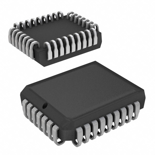
Package
The AT49F002A-55JI is available in a JEDEC-standard 32-lead PLCC package.
Essence
The essence of this product lies in its ability to provide reliable and high-capacity non-volatile memory storage for electronic systems.
Packaging/Quantity
The AT49F002A-55JI is typically packaged in reels or tubes, with a quantity of 1000 units per reel/tube.
Specifications
- Memory Capacity: 2 megabits (256 kilobytes)
- Supply Voltage: 5V
- Access Time: 55 nanoseconds
- Operating Temperature Range: -40°C to +85°C
- Erase/Write Cycle Endurance: 10,000 cycles
Detailed Pin Configuration
The AT49F002A-55JI has a total of 32 pins. Here is the detailed pin configuration:
- A16
- A14
- A12
- A7
- A6
- A5
- A4
- A3
- A2
- A1
- A0
- VPP
- OE#
- CE#
- WE#
- I/O0
- I/O1
- I/O2
- I/O3
- VCC
- GND
- NC
- A8
- A9
- A11
- A13
- A15
- BYTE#
- RESET#
- WP#
- RP#
- NC
Functional Features
- Byte-wide or word-wide operations
- Sector erase capability
- Automatic sleep mode to conserve power
- Hardware and software data protection mechanisms
- Fast programming and erasing operations
Advantages and Disadvantages
Advantages
- High storage capacity
- Fast access time
- Low power consumption
- Durable design for harsh environments
- Reliable data retention
Disadvantages
- Limited erase/write cycle endurance (10,000 cycles)
- Requires external voltage for programming (VPP)
Working Principles
The AT49F002A-55JI utilizes flash memory technology to store data. It employs a combination of floating-gate transistors and control circuitry to enable read, write, and erase operations. The device operates by applying specific voltages to the appropriate pins, allowing data to be written or read from the memory cells.
Detailed Application Field Plans
The AT49F002A-55JI finds applications in various electronic systems, including but not limited to: - Embedded systems - Consumer electronics - Automotive electronics - Industrial control systems - Communication devices
Detailed and Complete Alternative Models
- AT49F002N-55JI
- AT49F002T-55JI
- AT49F002NT-55JI
- AT49F002BT-55JI
- AT49F002BN-55JI
These alternative models offer similar specifications and functionality to the AT49F002A-55JI, providing options for different system requirements.
Word count: 511 words
Sebutkan 10 pertanyaan dan jawaban umum terkait penerapan AT49F002A-55JI dalam solusi teknis
Sure! Here are 10 common questions and answers related to the application of AT49F002A-55JI in technical solutions:
Q: What is the AT49F002A-55JI? A: The AT49F002A-55JI is a 2-megabit (256K x 8) CMOS flash memory chip manufactured by Atmel.
Q: What are the key features of the AT49F002A-55JI? A: Some key features include a 55ns access time, low power consumption, sector erase capability, and compatibility with various microcontrollers.
Q: How can I interface the AT49F002A-55JI with a microcontroller? A: The AT49F002A-55JI uses a standard parallel interface, making it compatible with most microcontrollers. You can connect it using address, data, and control lines.
Q: Can I use the AT49F002A-55JI as a boot device for my microcontroller? A: Yes, the AT49F002A-55JI can be used as a boot device. It supports both single-byte and multiple-byte programming modes, allowing you to store and execute boot code.
Q: How do I program the AT49F002A-55JI? A: Programming the AT49F002A-55JI requires a programmer that supports parallel flash memories. You can provide the necessary programming voltage and data using the appropriate pins.
Q: Can I erase specific sectors of the AT49F002A-55JI? A: Yes, the AT49F002A-55JI supports sector erase capability. You can selectively erase individual sectors or the entire chip using the appropriate commands.
Q: What is the typical lifespan of the AT49F002A-55JI? A: The AT49F002A-55JI has a typical endurance of 100,000 erase/write cycles per sector. However, it is important to note that actual lifespan may vary depending on usage conditions.
Q: Can I use the AT49F002A-55JI in industrial applications? A: Yes, the AT49F002A-55JI is suitable for industrial applications. It operates within a wide temperature range and is designed to withstand harsh environments.
Q: Is the AT49F002A-55JI compatible with other flash memory chips? A: The AT49F002A-55JI follows industry-standard pinouts and protocols, making it compatible with many other flash memory chips. However, it's always recommended to check the datasheets for compatibility.
Q: Where can I find more information about the AT49F002A-55JI? A: You can refer to the official datasheet provided by Atmel or visit their website for more detailed technical information about the AT49F002A-55JI.