

Lihat spesifikasi untuk detail produk.
MAX9034AUD-T
Product Overview
- Category: Integrated Circuit (IC)
- Use: Signal Amplification and Conditioning
- Characteristics: Low Power, High Precision, Wide Input Voltage Range
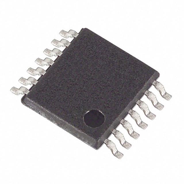
- Package: 8-pin µMAX®
- Essence: Operational Amplifier
- Packaging/Quantity: Tape and Reel (3000 units per reel)
Specifications
- Supply Voltage: 2.7V to 5.5V
- Input Offset Voltage: ±0.5mV (max)
- Input Bias Current: ±1nA (max)
- Gain Bandwidth Product: 1MHz (typ)
- Slew Rate: 0.6V/µs (typ)
- Operating Temperature Range: -40°C to +85°C
Pin Configuration
The MAX9034AUD-T has the following pin configuration:
```
| | --| IN- OUT |-- Pin 1: Output --| IN+ VCC |-- Pin 2: Positive Supply Voltage --| GND NC |-- Pin 3: Ground --| NC IN- |-- Pin 4: Negative Input --| NC IN+ |-- Pin 5: Positive Input --| NC GND |-- Pin 6: Ground --| NC NC |-- Pin 7: No Connection --| NC NC |-- Pin 8: No Connection |___________| ```
Functional Features
- Low input offset voltage for accurate signal amplification.
- Rail-to-rail input and output capability for wide dynamic range.
- Low power consumption for energy-efficient applications.
- High gain bandwidth product for precise signal conditioning.
- Stable operation over a wide temperature range.
Advantages and Disadvantages
Advantages: - Low power consumption extends battery life in portable devices. - Wide input voltage range allows for versatile applications. - High precision amplification ensures accurate signal processing.
Disadvantages: - Limited number of pins restricts the flexibility of the IC. - Not suitable for high-frequency applications due to limited bandwidth.
Working Principles
The MAX9034AUD-T is an operational amplifier that amplifies and conditions analog signals. It operates by taking the difference between the positive and negative input voltages and amplifying it with a high gain. The amplified output is then available at the output pin. The IC is designed to operate with low power consumption while maintaining high precision and stability over a wide temperature range.
Detailed Application Field Plans
The MAX9034AUD-T can be used in various applications, including but not limited to:
- Sensor Signal Conditioning: Amplifying and conditioning signals from sensors such as temperature, pressure, or light sensors.
- Audio Amplification: Amplifying audio signals in portable devices like smartphones or MP3 players.
- Industrial Control Systems: Signal conditioning for control systems in industrial automation.
- Medical Instrumentation: Precise signal amplification in medical devices for diagnostics or monitoring.
Detailed and Complete Alternative Models
- MAX9035AUD-T: Similar specifications and features, but with a different pin configuration.
- MAX9036AUD-T: Higher gain bandwidth product and lower input offset voltage compared to MAX9034AUD-T.
- MAX9037AUD-T: Lower power consumption and wider supply voltage range than MAX9034AUD-T.
These alternative models provide options with varying characteristics to suit different application requirements.
Word count: 314 words
Sebutkan 10 pertanyaan dan jawaban umum terkait penerapan MAX9034AUD-T dalam solusi teknis
Sure! Here are 10 common questions and answers related to the application of MAX9034AUD-T in technical solutions:
Q: What is the MAX9034AUD-T? A: The MAX9034AUD-T is a high-speed, low-power comparator IC (integrated circuit) designed for various applications in electronic systems.
Q: What is the operating voltage range of the MAX9034AUD-T? A: The operating voltage range of the MAX9034AUD-T is typically between 2.7V and 5.5V.
Q: What is the maximum input offset voltage of the MAX9034AUD-T? A: The maximum input offset voltage of the MAX9034AUD-T is typically ±1mV.
Q: Can the MAX9034AUD-T operate in both single-supply and dual-supply configurations? A: Yes, the MAX9034AUD-T can be used in both single-supply and dual-supply configurations, making it versatile for different applications.
Q: What is the typical response time of the MAX9034AUD-T? A: The typical response time of the MAX9034AUD-T is around 9ns, making it suitable for high-speed applications.
Q: Does the MAX9034AUD-T have built-in hysteresis? A: Yes, the MAX9034AUD-T features built-in hysteresis, which helps to improve noise immunity and stability in the presence of small input signal variations.
Q: Can the MAX9034AUD-T tolerate overvoltage conditions? A: Yes, the MAX9034AUD-T has built-in protection features that allow it to withstand overvoltage conditions up to 18V.
Q: What is the quiescent current consumption of the MAX9034AUD-T? A: The quiescent current consumption of the MAX9034AUD-T is typically around 1.5mA.
Q: Can the MAX9034AUD-T drive capacitive loads directly? A: Yes, the MAX9034AUD-T has a high output current capability, allowing it to drive capacitive loads up to 100pF without requiring additional buffering.
Q: What are some typical applications for the MAX9034AUD-T? A: The MAX9034AUD-T can be used in various applications such as level shifting, window comparators, motor control, power supply monitoring, and general-purpose signal conditioning.
Please note that the answers provided here are general and may vary depending on specific datasheet specifications and application requirements.