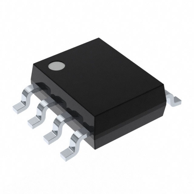
Lihat spesifikasi untuk detail produk.

MAX4274BJESA
Product Overview
- Category: Integrated Circuits (ICs)
- Use: Operational Amplifiers (Op Amps)
- Characteristics:
- High-speed, low-power, voltage-feedback operational amplifier
- Rail-to-rail input and output
- Single-supply operation from +2.7V to +5.5V
- Low distortion: THD+N = 0.0003% at 1kHz
- Package: 8-pin SOIC (Small Outline Integrated Circuit)
- Essence: MAX4274BJESA is a high-performance operational amplifier designed for various applications requiring precision amplification with low distortion.
Specifications
- Supply Voltage Range: +2.7V to +5.5V
- Input Offset Voltage: ±0.5mV (max)
- Gain Bandwidth Product: 50MHz
- Slew Rate: 30V/µs
- Input Bias Current: ±1nA (max)
- Output Current: ±60mA (max)
- Operating Temperature Range: -40°C to +125°C
Pin Configuration
The MAX4274BJESA has the following pin configuration:
```
| | --| IN- OUT |-- Pin 1: Inverting Input (-) --| IN+ VCC |-- Pin 2: Non-Inverting Input (+) --| VEE GND |-- Pin 3: Negative Power Supply --| NC NC |-- Pin 4: Not Connected --| NC NC |-- Pin 5: Not Connected --| VOUT VEE |-- Pin 6: Output --| NC NC |-- Pin 7: Not Connected --| NC NC |-- Pin 8: Not Connected |___________| ```
Functional Features
- High-speed amplification: The MAX4274BJESA offers a gain bandwidth product of 50MHz, making it suitable for applications requiring fast signal processing.
- Low distortion: With a total harmonic distortion plus noise (THD+N) of only 0.0003% at 1kHz, this operational amplifier ensures accurate amplification without introducing significant distortion.
- Rail-to-rail input and output: The device supports input and output signals that can swing close to the supply rails, allowing for maximum dynamic range and flexibility in various applications.
- Single-supply operation: The MAX4274BJESA operates from a single power supply voltage ranging from +2.7V to +5.5V, making it compatible with a wide range of systems.
Advantages and Disadvantages
Advantages: - High-speed amplification capability - Low distortion for accurate signal reproduction - Wide operating temperature range (-40°C to +125°C) - Rail-to-rail input and output for maximum dynamic range - Single-supply operation for compatibility with various systems
Disadvantages: - Limited number of pins for additional functionality - Not suitable for high-voltage applications
Working Principles
The MAX4274BJESA is based on a voltage-feedback architecture, utilizing a differential amplifier configuration to amplify the input signal. It employs internal compensation techniques to ensure stability and minimize phase shift. The rail-to-rail input and output stages allow for efficient signal handling near the supply rails, while the low distortion characteristics ensure faithful signal reproduction.
Application Field Plans
The MAX4274BJESA finds applications in various fields, including but not limited to: - Audio amplification - Sensor signal conditioning - Active filters - Data acquisition systems - Medical instrumentation - Industrial control systems
Alternative Models
- MAX4275BJESA: Similar specifications and features, but with a different pin configuration (14-pin SOIC package)
- MAX4276BJESA: Higher gain bandwidth product (100MHz) and lower input offset voltage (±0.2mV)
- MAX4277BJESA: Lower power consumption and wider supply voltage range (+2.5V to +5.5V)
These alternative models provide flexibility in choosing the most suitable operational amplifier based on specific application requirements.
Word count: 446 words
Sebutkan 10 pertanyaan dan jawaban umum terkait penerapan MAX4274BJESA dalam solusi teknis
Sure! Here are 10 common questions and answers related to the application of MAX4274BJESA in technical solutions:
Q: What is MAX4274BJESA? A: MAX4274BJESA is a high-speed, low-power operational amplifier designed for various technical applications.
Q: What is the voltage supply range for MAX4274BJESA? A: The voltage supply range for MAX4274BJESA is typically between +2.7V and +5.5V.
Q: What is the maximum output current of MAX4274BJESA? A: The maximum output current of MAX4274BJESA is typically ±50mA.
Q: Can MAX4274BJESA operate in single-supply mode? A: Yes, MAX4274BJESA can operate in both single-supply and dual-supply modes.
Q: What is the bandwidth of MAX4274BJESA? A: The bandwidth of MAX4274BJESA is typically 100MHz.
Q: Is MAX4274BJESA suitable for precision applications? A: No, MAX4274BJESA is not specifically designed for precision applications due to its moderate input offset voltage.
Q: Can MAX4274BJESA drive capacitive loads? A: Yes, MAX4274BJESA has a high slew rate and can drive capacitive loads up to a certain limit.
Q: What is the input voltage range of MAX4274BJESA? A: The input voltage range of MAX4274BJESA is typically between -0.3V and Vcc+0.3V.
Q: Does MAX4274BJESA have thermal shutdown protection? A: No, MAX4274BJESA does not have built-in thermal shutdown protection.
Q: What are some typical applications of MAX4274BJESA? A: Some typical applications of MAX4274BJESA include active filters, data acquisition systems, and signal conditioning circuits.
Please note that the answers provided here are general and may vary depending on the specific datasheet and application requirements.

