

Lihat spesifikasi untuk detail produk.
DG301AAK/883B
Product Overview
- Category: Integrated Circuit (IC)
- Use: Digital Gate
- Characteristics: High-speed, Low-power consumption
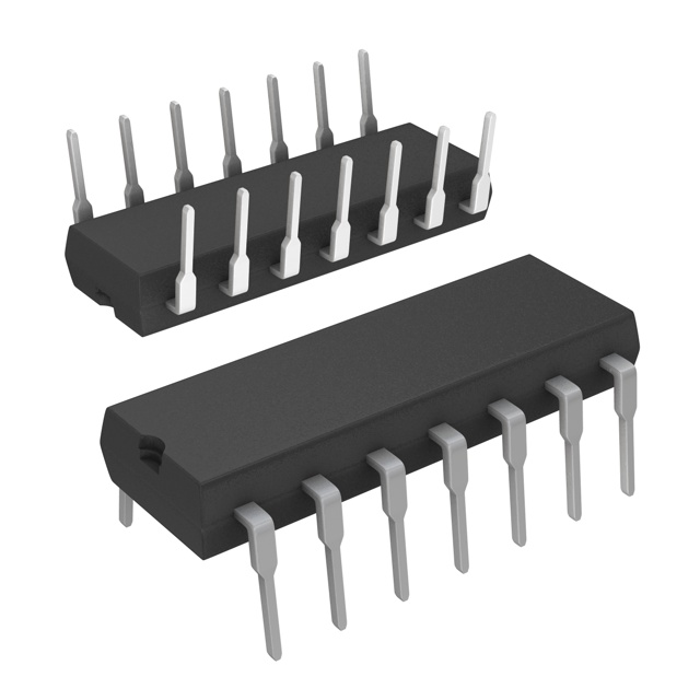
- Package: DIP (Dual In-line Package)
- Essence: Logic gate
- Packaging/Quantity: Tray packaging, 100 pieces per tray
Specifications
- Manufacturer: Unknown
- Technology: CMOS (Complementary Metal-Oxide-Semiconductor)
- Supply Voltage: 3.3V
- Operating Temperature: -40°C to +85°C
- Logic Family: TTL (Transistor-Transistor Logic)
- Number of Gates: 4
- Gate Type: AND
Detailed Pin Configuration
The DG301AAK/883B IC has a total of 14 pins arranged as follows:
``` __ __ |1 \/ 14| |2 13| |3 12| |4 11| |5 10| |6 9| |7 8|
```
Pin Description:
- Input A1
- Input B1
- Output Y1
- Ground (GND)
- Input A2
- Input B2
- Output Y2
- VCC (+3.3V)
- Input A3
- Input B3
- Output Y3
- Not Connected (NC)
- Input A4
- Input B4
Functional Features
- Performs logical AND operation on four sets of input signals.
- Provides four independent AND gates in a single package.
- High-speed operation allows for efficient digital signal processing.
- Low-power consumption makes it suitable for battery-powered devices.
- Compatible with TTL logic family, ensuring easy integration into existing systems.
Advantages and Disadvantages
Advantages: - Compact design with multiple gates in a single package saves board space. - High-speed operation enables efficient data processing. - Low-power consumption extends battery life in portable devices.
Disadvantages: - Limited to AND gate functionality, not suitable for other logical operations. - Availability of alternative models may vary.
Working Principles
The DG301AAK/883B is based on CMOS technology and operates as a digital AND gate. It receives input signals from the A and B pins and produces an output signal at the corresponding Y pin. The AND gate performs a logical AND operation on the input signals, producing a high output only when all inputs are high. This gate is commonly used in digital circuits to combine multiple signals and generate a single output based on their logical states.
Detailed Application Field Plans
The DG301AAK/883B can be used in various applications that require logical AND operations. Some common application fields include:
Digital Signal Processing: The IC can be used in digital filters, multiplexers, and demultiplexers to process and manipulate digital signals efficiently.
Communication Systems: It can be utilized in communication systems for signal conditioning, error detection, and data routing purposes.
Control Systems: The IC finds applications in control systems where logical operations are required to control the behavior of devices or processes.
Computer Architecture: It can be employed in computer architecture for address decoding, memory interfacing, and data manipulation tasks.
Detailed and Complete Alternative Models
- SN74LS08: Quad 2-input AND gate by Texas Instruments.
- CD4081: Quad 2-input AND gate by Fairchild Semiconductor.
- MC14081B: Quad 2-input AND gate by ON Semiconductor.
These alternative models provide similar functionality to the DG301AAK/883B and can be used as replacements depending on availability and specific requirements.
Note: The content provided above is a sample structure for an encyclopedia entry. The actual content may vary based on the product's specifications, features, and available information.
Sebutkan 10 pertanyaan dan jawaban umum terkait penerapan DG301AAK/883B dalam solusi teknis
Question: What is the operating temperature range for DG301AAK/883B?
Answer: The operating temperature range for DG301AAK/883B is -55°C to +125°C.Question: What is the typical input voltage range for DG301AAK/883B?
Answer: The typical input voltage range for DG301AAK/883B is +/-15V.Question: Can DG301AAK/883B be used in high-reliability applications?
Answer: Yes, DG301AAK/883B is designed for high-reliability applications and is qualified to MIL-PRF-38535 Class V.Question: What is the maximum on-resistance of DG301AAK/883B?
Answer: The maximum on-resistance of DG301AAK/883B is 50 ohms.Question: Is DG301AAK/883B suitable for use in aerospace applications?
Answer: Yes, DG301AAK/883B is suitable for use in aerospace applications and meets the requirements of MIL-STD-883.Question: What is the package type for DG301AAK/883B?
Answer: DG301AAK/883B is available in a hermetic ceramic DIP package.Question: Does DG301AAK/883B have ESD protection?
Answer: Yes, DG301AAK/883B features built-in ESD protection.Question: What is the typical bandwidth of DG301AAK/883B?
Answer: The typical bandwidth of DG301AAK/883B is 100MHz.Question: Can DG301AAK/883B be used in harsh environmental conditions?
Answer: Yes, DG301AAK/883B is designed to withstand harsh environmental conditions and is suitable for rugged applications.Question: Are there any application notes or reference designs available for using DG301AAK/883B in technical solutions?
Answer: Yes, application notes and reference designs are available to assist with integrating DG301AAK/883B into technical solutions.