

Lihat spesifikasi untuk detail produk.
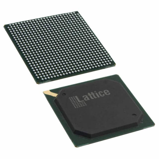
LFE2M50E-6F672C
Product Overview
Category
The LFE2M50E-6F672C belongs to the category of Field Programmable Gate Arrays (FPGAs).
Use
FPGAs are integrated circuits that can be programmed and reprogrammed to perform various digital functions. The LFE2M50E-6F672C is specifically designed for applications requiring high-performance and low-power consumption.
Characteristics
- High-performance FPGA with low power consumption
- Programmable and reprogrammable
- Offers flexibility in designing digital circuits
- Suitable for a wide range of applications
Package
The LFE2M50E-6F672C comes in a compact package, ensuring easy integration into electronic systems.
Essence
The essence of the LFE2M50E-6F672C lies in its ability to provide a customizable and efficient solution for digital circuit design.
Packaging/Quantity
The LFE2M50E-6F672C is typically packaged individually and is available in various quantities depending on the requirements of the user.
Specifications
- Model: LFE2M50E-6F672C
- Family: Lattice ECP2M
- Logic Elements: 50,000
- Speed Grade: 6
- Package: 672-ball FineLine BGA
- Operating Voltage: 1.2V
- I/O Pins: 400
- RAM Bits: 1,152 Kbits
- Embedded Multipliers: 96
- Maximum Frequency: 400 MHz
Detailed Pin Configuration
The LFE2M50E-6F672C has a total of 400 I/O pins, each serving a specific purpose in the circuit design. A detailed pin configuration diagram can be found in the product datasheet.
Functional Features
- High-performance FPGA with low power consumption
- Flexible and customizable digital circuit design
- Support for various communication protocols
- Embedded multipliers for efficient mathematical operations
- On-chip memory for data storage
- Built-in security features for protecting intellectual property
Advantages and Disadvantages
Advantages
- High-performance capabilities
- Low power consumption
- Flexibility in circuit design
- Support for various communication protocols
- Efficient mathematical operations with embedded multipliers
- On-chip memory for data storage
- Built-in security features
Disadvantages
- Limited logic elements compared to larger FPGAs
- Higher cost compared to simpler programmable logic devices
Working Principles
The LFE2M50E-6F672C operates based on the principles of reconfigurable computing. It consists of a matrix of configurable logic blocks interconnected through programmable routing resources. The user can program the FPGA using hardware description languages or graphical tools to define the desired functionality.
Detailed Application Field Plans
The LFE2M50E-6F672C finds applications in various fields, including:
- Telecommunications: Used in base stations, routers, and network switches for high-speed data processing.
- Industrial Automation: Employed in control systems, robotics, and machine vision applications for real-time data processing and control.
- Automotive: Utilized in advanced driver-assistance systems (ADAS), infotainment systems, and engine control units (ECUs) for enhanced performance and functionality.
- Aerospace and Defense: Integrated into radar systems, avionics, and military communication equipment for reliable and secure operation.
- Medical Devices: Incorporated into medical imaging systems, patient monitoring devices, and laboratory equipment for accurate data processing and analysis.
Detailed and Complete Alternative Models
- Xilinx Virtex UltraScale+ VU9P: Offers higher logic capacity and performance.
- Intel Stratix 10 GX: Provides advanced features and high-speed interfaces.
- Microsemi PolarFire FPGA: Known for its low power consumption and security features.
- QuickLogic EOS S3: Offers ultra-low power consumption for battery-operated applications.
These alternative models provide different options with varying capabilities to suit specific project requirements.
In conclusion, the LFE2M50E-6F672C is a high-performance FPGA that offers flexibility, low power consumption, and a wide range of applications. Its customizable nature and embedded features make it an ideal choice for various digital circuit designs.
Sebutkan 10 pertanyaan dan jawaban umum terkait penerapan LFE2M50E-6F672C dalam solusi teknis
Sure! Here are 10 common questions and answers related to the application of LFE2M50E-6F672C in technical solutions:
Q: What is the LFE2M50E-6F672C? A: The LFE2M50E-6F672C is a specific model of Field-Programmable Gate Array (FPGA) manufactured by Lattice Semiconductor.
Q: What are the key features of the LFE2M50E-6F672C? A: Some key features of this FPGA include 50,000 Look-Up Tables (LUTs), 672 user I/O pins, low power consumption, and high-speed performance.
Q: What are the typical applications of the LFE2M50E-6F672C? A: This FPGA is commonly used in various technical solutions such as industrial automation, telecommunications, automotive electronics, medical devices, and more.
Q: How can I program the LFE2M50E-6F672C? A: The LFE2M50E-6F672C can be programmed using hardware description languages (HDLs) like VHDL or Verilog, along with specialized software tools provided by Lattice Semiconductor.
Q: Can I reprogram the LFE2M50E-6F672C after it has been deployed in a solution? A: Yes, FPGAs like the LFE2M50E-6F672C are designed to be reprogrammable, allowing for flexibility and updates even after deployment.
Q: What are the advantages of using the LFE2M50E-6F672C in technical solutions? A: Some advantages include its ability to handle complex logic functions, its flexibility for customization, and its suitability for prototyping and low-volume production.
Q: Are there any limitations or considerations when using the LFE2M50E-6F672C? A: Some considerations include power consumption, heat dissipation, and the need for proper signal integrity and timing analysis during design.
Q: Can the LFE2M50E-6F672C interface with other components or devices in a solution? A: Yes, the FPGA can interface with various components and devices through its user I/O pins, allowing for integration with sensors, actuators, memory, communication interfaces, and more.
Q: Are there any development boards or evaluation kits available for the LFE2M50E-6F672C? A: Yes, Lattice Semiconductor provides development boards and evaluation kits specifically designed for the LFE2M50E-6F672C, which can aid in prototyping and testing.
Q: Where can I find technical documentation and support for the LFE2M50E-6F672C? A: Technical documentation, datasheets, application notes, and support resources can be found on the official website of Lattice Semiconductor or by contacting their customer support team.
Please note that the specific details and answers may vary depending on the manufacturer's documentation and guidelines.