

Lihat spesifikasi untuk detail produk.
LFE2M50E-5F484I
Product Overview
Category
The LFE2M50E-5F484I belongs to the category of Field-Programmable Gate Arrays (FPGAs).
Use
This FPGA is commonly used in various electronic devices and systems for digital logic implementation, prototyping, and hardware acceleration.
Characteristics
- High-performance programmable logic device
- Offers flexibility and reconfigurability
- Provides a large number of configurable logic blocks (CLBs) and input/output (I/O) pins
- Supports complex digital designs and algorithms
- Enables rapid development and customization of electronic systems
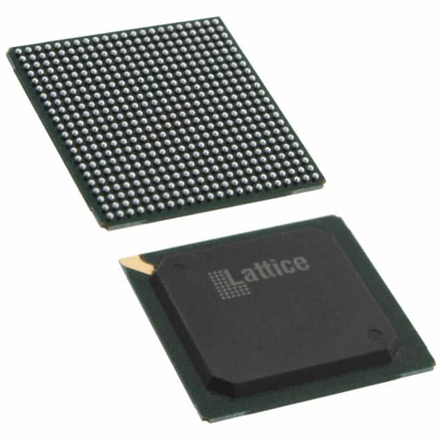
Package
The LFE2M50E-5F484I comes in a compact and durable package suitable for surface-mount technology (SMT) assembly.
Essence
The essence of this FPGA lies in its ability to provide a versatile platform for implementing complex digital circuits with high performance and flexibility.
Packaging/Quantity
The LFE2M50E-5F484I is typically packaged in reels or trays, containing a specific quantity of units per package. The exact packaging and quantity may vary depending on the manufacturer's specifications.
Specifications
- Device family: Lattice ECP2M
- Logic elements: 50,000
- Number of I/O pins: 484
- Operating voltage: 1.2V
- Maximum operating frequency: 500 MHz
- Embedded memory: Up to 4.8 Mb
- Programmable interconnect resources: Abundant routing resources for flexible connectivity
Detailed Pin Configuration
The LFE2M50E-5F484I has a well-defined pin configuration that facilitates easy integration into electronic systems. The detailed pin configuration can be found in the product datasheet provided by the manufacturer.
Functional Features
- High-speed and low-power operation
- Support for various I/O standards and protocols
- On-chip PLLs for clock management and synchronization
- Dedicated DSP blocks for efficient digital signal processing
- Built-in memory blocks for data storage and retrieval
- Flexible configuration options for optimal resource utilization
Advantages and Disadvantages
Advantages
- Versatile and flexible platform for digital logic implementation
- Rapid prototyping and development of electronic systems
- High-performance computing capabilities
- Reconfigurable nature allows for iterative design improvements
- Availability of abundant resources for complex designs
Disadvantages
- Steep learning curve for beginners due to the complexity of FPGA programming
- Higher cost compared to traditional fixed-function integrated circuits
- Limited support for analog circuitry
Working Principles
The LFE2M50E-5F484I operates based on the principles of reconfigurable computing. It consists of configurable logic blocks (CLBs), interconnect resources, I/O pins, and other specialized components. The device can be programmed using hardware description languages (HDL) or graphical tools to define the desired digital circuit functionality. Upon programming, the FPGA configures its internal resources to implement the specified logic, enabling the system to perform the desired operations.
Detailed Application Field Plans
The LFE2M50E-5F484I finds applications in various fields, including:
- Communications: Used in networking equipment, routers, and switches for high-speed data processing and protocol handling.
- Aerospace and Defense: Employed in radar systems, avionics, and military communication devices for their high-performance computing capabilities.
- Industrial Automation: Utilized in programmable logic controllers (PLCs) and industrial control systems for real-time control and monitoring.
- Medical Devices: Integrated into medical imaging systems, patient monitoring devices, and diagnostic equipment for advanced signal processing and data analysis.
- Automotive: Incorporated in automotive electronics for functions like engine control, driver assistance systems, and infotainment.
Detailed and Complete Alternative Models
- Xilinx Virtex-7 XC7VX485T: A comparable FPGA with similar logic capacity and performance characteristics.
- Intel Cyclone V EP4CE115F29C7: An alternative FPGA offering a different architecture but similar capabilities.
- Microsemi SmartFusion2 M2S050T: A mixed-signal FPGA that combines programmable logic with integrated ARM Cortex-M3 processor.
These alternative models provide similar functionality and can be considered as substitutes based on specific project requirements.
In conclusion, the LFE2M50E-5F484I is a high-performance FPGA that offers flexibility, reconfigurability, and abundant resources for implementing complex digital circuits. Its applications span across various industries, and it has several alternative models available in the market to cater to diverse project needs.
Sebutkan 10 pertanyaan dan jawaban umum terkait penerapan LFE2M50E-5F484I dalam solusi teknis
Sure! Here are 10 common questions and answers related to the application of LFE2M50E-5F484I in technical solutions:
Q: What is the LFE2M50E-5F484I? A: The LFE2M50E-5F484I is a specific model of Field-Programmable Gate Array (FPGA) manufactured by Lattice Semiconductor.
Q: What are the key features of the LFE2M50E-5F484I? A: The LFE2M50E-5F484I offers 50,000 Look-Up Tables (LUTs), 1,280 kilobits of embedded memory, and 120 programmable input/output pins.
Q: What are some typical applications for the LFE2M50E-5F484I? A: The LFE2M50E-5F484I is commonly used in various technical solutions such as industrial automation, telecommunications, automotive electronics, and medical devices.
Q: How can I program the LFE2M50E-5F484I? A: The LFE2M50E-5F484I can be programmed using Lattice Diamond or Lattice Radiant software tools provided by Lattice Semiconductor.
Q: Can the LFE2M50E-5F484I be reprogrammed after deployment? A: Yes, the LFE2M50E-5F484I is a reprogrammable FPGA, allowing for flexibility and updates even after it has been deployed in a technical solution.
Q: What are the power requirements for the LFE2M50E-5F484I? A: The LFE2M50E-5F484I typically operates at a voltage range of 1.14V to 1.26V, with power consumption varying based on the design and usage.
Q: Can the LFE2M50E-5F484I interface with other components or devices? A: Yes, the LFE2M50E-5F484I supports various communication protocols such as SPI, I2C, UART, and Ethernet, allowing for seamless integration with other components or devices.
Q: What are the temperature specifications for the LFE2M50E-5F484I? A: The LFE2M50E-5F484I is designed to operate within a temperature range of -40°C to 100°C, making it suitable for both industrial and commercial applications.
Q: Are there any development boards available for the LFE2M50E-5F484I? A: Yes, Lattice Semiconductor provides development boards like the LFE2M50E-5F484I-DB1, which can be used for prototyping and evaluation purposes.
Q: Where can I find additional technical documentation and support for the LFE2M50E-5F484I? A: You can find detailed technical documentation, datasheets, application notes, and support resources on the official website of Lattice Semiconductor or by contacting their customer support team.
Please note that the answers provided here are general and may vary depending on specific requirements and use cases.