

Lihat spesifikasi untuk detail produk.
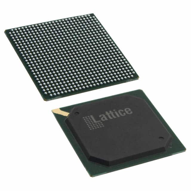
LFE2M35SE-6F672C
Product Overview
Category
The LFE2M35SE-6F672C belongs to the category of Field Programmable Gate Arrays (FPGAs).
Use
FPGAs are integrated circuits that can be programmed and reprogrammed to perform various digital functions. The LFE2M35SE-6F672C is specifically designed for applications requiring high-performance and low-power consumption.
Characteristics
- High performance: The LFE2M35SE-6F672C offers a high logic density and fast processing capabilities, making it suitable for complex digital designs.
- Low power consumption: This FPGA is designed to minimize power consumption, making it energy-efficient and suitable for battery-powered devices.
- Programmability: The LFE2M35SE-6F672C can be easily programmed and reconfigured to adapt to different application requirements.
- Versatility: It supports a wide range of digital functions, including data processing, signal generation, and control logic implementation.
Package and Quantity
The LFE2M35SE-6F672C is available in a compact package, typically a plastic ball grid array (BGA). The exact dimensions and pin count may vary depending on the specific package variant. It is usually sold individually or in small quantities.
Specifications
- FPGA Family: Lattice ECP2M
- Logic Elements: 35,000
- Speed Grade: -6
- Package Type: BGA
- Package Pins: 672
- Operating Voltage: 1.2V
- Maximum Frequency: 400 MHz
- I/O Standards: LVCMOS, LVTTL, SSTL, HSTL, LVDS, RSDS, LVPECL, CML
Detailed Pin Configuration
The LFE2M35SE-6F672C has 672 pins, each serving a specific purpose in the FPGA's operation. The pin configuration includes input/output (I/O) pins, power supply pins, ground pins, and configuration pins. A detailed pinout diagram can be found in the product datasheet.
Functional Features
- High-speed data processing: The LFE2M35SE-6F672C can handle complex digital operations at high speeds, making it suitable for applications requiring real-time data processing.
- Flexible I/O capabilities: It supports various I/O standards, allowing seamless integration with different external devices and interfaces.
- Embedded memory blocks: The FPGA includes dedicated memory blocks that can be used for storing data or implementing lookup tables, enhancing its versatility.
- Clock management: The LFE2M35SE-6F672C provides advanced clocking features, including phase-locked loops (PLLs) and delay-locked loops (DLLs), enabling precise timing control.
Advantages and Disadvantages
Advantages
- High performance and logic density
- Low power consumption
- Programmability and reconfigurability
- Versatility in supporting multiple I/O standards
- Advanced clock management capabilities
Disadvantages
- Relatively higher cost compared to other programmable logic devices
- Steeper learning curve for programming and utilizing the full potential of the FPGA
Working Principles
The LFE2M35SE-6F672C operates based on the principles of configurable logic. It consists of an array of programmable logic elements interconnected through configurable routing resources. These logic elements can be programmed to implement desired digital functions by configuring their interconnections and behavior using hardware description languages (HDLs) or graphical design tools. Once programmed, the FPGA executes the desired functionality by routing signals through the configured logic elements.
Detailed Application Field Plans
The LFE2M35SE-6F672C finds applications in various fields, including:
- Communications: It can be used for implementing signal processing algorithms, protocol converters, and high-speed data interfaces.
- Industrial automation: The FPGA can be utilized for control systems, motor drives, and sensor interfacing.
- Aerospace and defense: It is suitable for radar systems, avionics, and secure communication systems.
- Medical devices: The FPGA can be employed in medical imaging, patient monitoring, and diagnostic equipment.
- Internet of Things (IoT): It can enable edge computing, sensor fusion, and data analytics in IoT applications.
Detailed and Complete Alternative Models
- LFE2M35SE-6F672I
- LFE2M35SE-7F672C
- LFE2M35SE-8F672C
- LFE2M35SE-6FN672C
- LFE2M35SE-6TN672C
These alternative models offer similar functionality and performance characteristics to the LFE2M35SE-6F672C but may differ in terms of speed grade, package type, or pin count.
In conclusion,
Sebutkan 10 pertanyaan dan jawaban umum terkait penerapan LFE2M35SE-6F672C dalam solusi teknis
Sure! Here are 10 common questions and answers related to the application of LFE2M35SE-6F672C in technical solutions:
Q: What is the LFE2M35SE-6F672C? A: The LFE2M35SE-6F672C is a specific model of Field-Programmable Gate Array (FPGA) manufactured by Lattice Semiconductor.
Q: What are the key features of the LFE2M35SE-6F672C? A: Some key features of this FPGA include 35,000 Look-Up Tables (LUTs), 672 user I/O pins, 6-input function capability, and support for various communication protocols.
Q: In what applications can the LFE2M35SE-6F672C be used? A: This FPGA can be used in a wide range of applications such as industrial automation, telecommunications, automotive electronics, medical devices, and more.
Q: How can I program the LFE2M35SE-6F672C? A: The LFE2M35SE-6F672C can be programmed using hardware description languages (HDLs) like VHDL or Verilog, which allow you to describe the desired functionality of the FPGA.
Q: What development tools are available for working with the LFE2M35SE-6F672C? A: Lattice Semiconductor provides software tools like Lattice Diamond or Lattice Radiant, which offer design entry, synthesis, simulation, and programming capabilities for their FPGAs.
Q: Can the LFE2M35SE-6F672C interface with other components or devices? A: Yes, the FPGA has a large number of user I/O pins that can be configured to interface with various components or devices such as sensors, actuators, memory modules, and communication interfaces.
Q: What are the power requirements for the LFE2M35SE-6F672C? A: The specific power requirements can vary depending on the application and design, but typically, this FPGA operates at a voltage range of 1.2V to 3.3V.
Q: Can the LFE2M35SE-6F672C be reprogrammed after deployment? A: Yes, FPGAs like the LFE2M35SE-6F672C are known for their reprogrammability, allowing you to modify the functionality of the device even after it has been deployed in a system.
Q: Are there any limitations or considerations when using the LFE2M35SE-6F672C? A: Some considerations include power consumption, timing constraints, and resource utilization. It's important to carefully plan and optimize your design to make the most efficient use of the FPGA resources.
Q: Where can I find additional documentation and support for the LFE2M35SE-6F672C? A: Lattice Semiconductor provides datasheets, user guides, application notes, and technical support through their website. You can also find online communities and forums where FPGA enthusiasts share knowledge and experiences.