

Lihat spesifikasi untuk detail produk.
CY7C1370BV25-167AC
Product Overview
Category
The CY7C1370BV25-167AC belongs to the category of integrated circuits (ICs).
Use
This IC is commonly used in electronic devices for various applications, including data storage, communication systems, and digital signal processing.
Characteristics
- High performance: The CY7C1370BV25-167AC offers high-speed data transfer and processing capabilities.
- Low power consumption: It is designed to operate efficiently with minimal power requirements.
- Compact package: The IC is available in a small form factor, making it suitable for space-constrained applications.
- Reliable operation: It ensures stable and reliable performance even under challenging conditions.
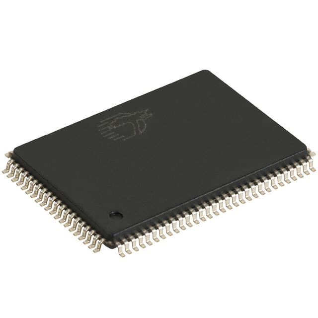
Package
The CY7C1370BV25-167AC is typically packaged in a compact and durable plastic casing. This package provides protection against external factors such as moisture, dust, and physical damage.
Essence
The essence of the CY7C1370BV25-167AC lies in its ability to process and store data efficiently, enabling seamless operation of electronic devices.
Packaging/Quantity
This IC is usually sold in reels or trays, with each reel or tray containing a specific quantity of units. The exact packaging and quantity may vary depending on the supplier or manufacturer.
Specifications
- Model: CY7C1370BV25-167AC
- Operating Voltage: 3.3V
- Speed: 167 MHz
- Memory Capacity: Varies (depending on specific model)
- Interface: Parallel
- Pin Count: 100
- Temperature Range: -40°C to +85°C
Detailed Pin Configuration
The CY7C1370BV25-167AC features a total of 100 pins, each serving a specific purpose. The pin configuration is as follows:
(Pin Number) - (Pin Name) - (Function) 1 - VDD - Power Supply 2 - GND - Ground 3 - A0-A18 - Address Inputs 4 - DQ0-DQ15 - Data Inputs/Outputs 5 - WE - Write Enable 6 - OE - Output Enable 7 - CE - Chip Enable 8 - RDY/BUSY - Ready/Busy Indicator 9 - CLK - Clock Input 10 - RESET - Reset Input ...
Functional Features
The CY7C1370BV25-167AC offers several functional features that enhance its performance and usability:
- High-speed data transfer: The IC enables rapid data transfer between different components, ensuring efficient communication within electronic devices.
- Flexible addressing: With a wide range of address inputs, the IC allows for versatile memory addressing schemes, accommodating various application requirements.
- Reliable data storage: It provides reliable and secure data storage capabilities, ensuring the integrity and availability of stored information.
- Low power consumption: The IC is designed to operate with minimal power consumption, making it suitable for battery-powered devices.
- Easy integration: Its compact package and standardized pin configuration facilitate easy integration into existing electronic systems.
Advantages and Disadvantages
Advantages
- High-performance data processing and storage capabilities
- Compact form factor for space-constrained applications
- Low power consumption for energy-efficient operation
- Versatile addressing options for flexible usage
- Reliable and secure data storage
Disadvantages
- Limited memory capacity compared to some alternative models
- Higher cost compared to lower-end ICs with similar functionalities
Working Principles
The CY7C1370BV25-167AC operates based on the principles of digital logic and memory storage. It utilizes integrated circuit technology to process and store data efficiently. The IC's internal architecture consists of various components such as registers, multiplexers, decoders, and memory cells. These components work together to enable data transfer, storage, and retrieval operations.
Detailed Application Field Plans
The CY7C1370BV25-167AC finds applications in various fields, including:
- Data storage devices: It is commonly used in solid-state drives (SSDs), memory cards, and USB flash drives for efficient data storage and retrieval.
- Communication systems: The IC is utilized in networking equipment, routers, and switches to facilitate high-speed data transfer and processing.
- Digital signal processing: It plays a crucial role in audio and video processing systems, enabling real-time data manipulation and analysis.
- Industrial automation: The IC is employed in industrial control systems, robotics, and automation equipment to ensure reliable and efficient operation.
Detailed and Complete Alternative Models
- CY7C1370BV25-200AC: Similar to the CY7C1370BV25-167AC, but with a higher operating speed of 200 MHz.
- CY7C1370BV25-133AC: Similar to the CY7C1370BV25-167AC, but with a lower operating speed of 133 MHz
Sebutkan 10 pertanyaan dan jawaban umum terkait penerapan CY7C1370BV25-167AC dalam solusi teknis
Sure! Here are 10 common questions and answers related to the application of CY7C1370BV25-167AC in technical solutions:
Question: What is the CY7C1370BV25-167AC?
Answer: The CY7C1370BV25-167AC is a specific model of a high-performance synchronous SRAM (Static Random Access Memory) chip.Question: What is the capacity of the CY7C1370BV25-167AC?
Answer: The CY7C1370BV25-167AC has a capacity of 128 megabits (Mb).Question: What is the operating voltage range for this chip?
Answer: The operating voltage range for the CY7C1370BV25-167AC is typically between 2.375V and 2.625V.Question: What is the maximum clock frequency supported by this chip?
Answer: The CY7C1370BV25-167AC supports a maximum clock frequency of 167 MHz.Question: What is the access time of this SRAM chip?
Answer: The access time of the CY7C1370BV25-167AC is 25 ns, meaning it takes 25 nanoseconds to read or write data.Question: Can this chip be used in industrial applications?
Answer: Yes, the CY7C1370BV25-167AC is designed to meet the requirements of industrial applications.Question: Does this chip have any built-in error correction capabilities?
Answer: No, the CY7C1370BV25-167AC does not have built-in error correction capabilities.Question: What is the package type of this chip?
Answer: The CY7C1370BV25-167AC is available in a 165-ball BGA (Ball Grid Array) package.Question: Can this chip be used in automotive applications?
Answer: Yes, the CY7C1370BV25-167AC is qualified for automotive applications and meets the AEC-Q100 standard.Question: What are some typical applications of the CY7C1370BV25-167AC?
Answer: The CY7C1370BV25-167AC can be used in various applications such as networking equipment, telecommunications systems, industrial automation, and automotive electronics.
Please note that these answers are based on general information about the CY7C1370BV25-167AC and may vary depending on specific requirements and use cases.